- 您现在的位置:买卖IC网 > PDF目录2009 > MAX3992UTG+T (Maxim Integrated Products)IC DATA RECOVERY W/EQ 24-TQFN PDF资料下载
参数资料
| 型号: | MAX3992UTG+T |
| 厂商: | Maxim Integrated Products |
| 文件页数: | 11/12页 |
| 文件大小: | 0K |
| 描述: | IC DATA RECOVERY W/EQ 24-TQFN |
| 标准包装: | 2,500 |
| 类型: | 时钟和数据恢复(CDR) |
| PLL: | 是 |
| 主要目的: | SONET/SDH.XFP 光学接收器 |
| 输入: | CML |
| 输出: | CML |
| 电路数: | 1 |
| 比率 - 输入:输出: | 1:2 |
| 差分 - 输入:输出: | 是/是 |
| 频率 - 最大: | 693.5MHz |
| 电源电压: | 3 V ~ 3.6 V |
| 工作温度: | 0°C ~ 85°C |
| 安装类型: | 表面贴装 |
| 封装/外壳: | 24-WFQFN 裸露焊盘 |
| 供应商设备封装: | 24-TQFN-EP(4x4) |
| 包装: | 带卷 (TR) |
MAX3992
Detailed Description
The MAX3992 clock and data recovery with equalizer
recovers data from the XFI interface. It consists of an
equalizer with LOS power detector and a data retimer
with LOL indicator. An optional recovered clock may
also be enabled for performance testing.
Equalizer
The SDI inputs of the MAX3992 accept serial NRZ data
from XFI standard interfaces. When signals from
400mVP-P to 1000mVP-P are applied to a transmission
line from 0 to 12 inches of FR-4, the equalizer restores
them for recovery by the CDR. The equalizer removes
most of the deterministic jitter caused by frequency
dependent skin effect and dielectric losses, as well as
connector loss.
PLL Retimer
The integrated PLL recovers a synchronous clock that
is used to retime the input data. Connect a 0.047F
capacitor between CFIL and VCC to provide PLL damp-
ening. The external reference connected to REFCLK
aids in frequency acquisition. Because the reference
clock is only used for frequency acquisition, an
extremely low jitter generation can be achieved from a
low-quality reference clock. The reference clock should
be within ±100ppm of the bit rate divided by 16 or 64.
10Gbps Clock and Data Recovery
with Equalizer
8
_______________________________________________________________________________________
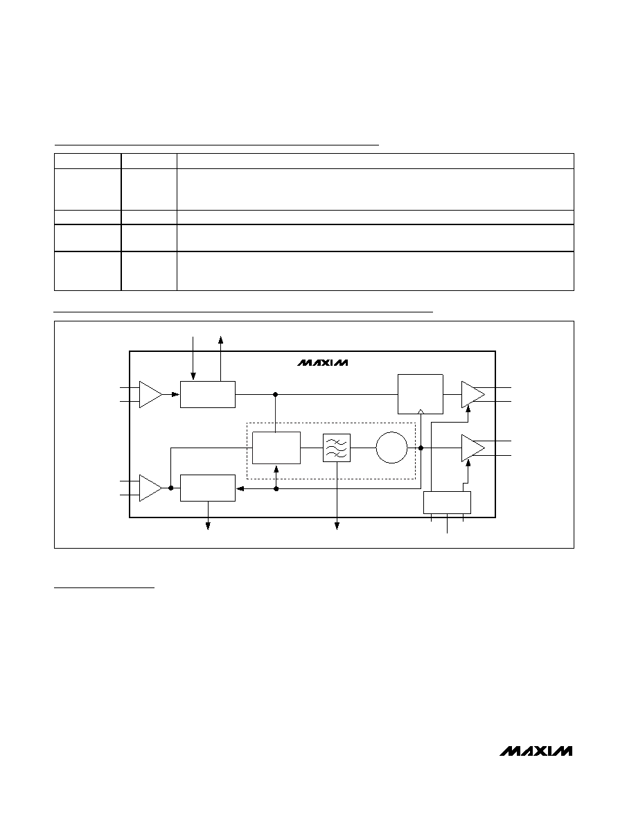
Figure 3. Functional Diagram
Functional Diagram
MAX3992
VTH
EQUALIZER
VCO
DFF
DQ
CML
PHASE/
FREQUENCY
DETECTOR
LOL
DETECTOR
LOS
LOL
FUNCTIONAL
CONTROL
CFIL
CML
SDI+
SDI-
REFCLK+
REFCLK-
SDO+
SDO-
SCLKO+
SCLKO-
FCTL1
FCTL2
PLL
200
POL
Pin Description (continued)
PIN
NAME
FUNCTION
22
REFCLK-
Negative Reference Clock Input, Digital. The REFCLK inputs are designed to be AC-coupled to the
reference clock source. REFCLK± have a 200
differential impedance. See the Detailed Description
section for more information. See Table 2.
23
FCTL1
Function Control Input 1, TTL. See Table 3 for more information.
24
VTH
LOS Threshold Input, Analog. A voltage applied to this input sets the LOS assert threshold. The LOS
power detector can be disabled if VTH is connected to VCC, which forces LOS low.
EP
Exposed
Pad
Supply Ground. The exposed pad must be soldered to the circuit-board ground for proper thermal
and electrical performance. The MAX3992 uses exposed-pad variation T2444-4 in the package
outline drawing. See the exposed-pad package.
相关PDF资料 |
PDF描述 |
|---|---|
| MAX504EPD+ | IC DAC 10BIT 5V LP SER 14-DIP |
| MAX507AENG+ | IC DAC 12BIT W/REF 24-DIP |
| MAX5100AEUP+T | IC DAC 8BIT QUAD R-R 20TSSOP |
| MAX5101BEUE+ | IC DAC 8BIT TRPL R-R 16-TSSOP |
| MAX5102AEUE+T | IC DAC 8BIT DUAL PAR-IN 16-TSSOP |
相关代理商/技术参数 |
参数描述 |
|---|---|
| MAX3996CGP | 功能描述:激光驱动器 3-5.5V 2.5Gbps VCSEL & Laser Driver RoHS:否 制造商:Micrel 数据速率:4.25 Gbps 工作电源电压:3 V to 3.6 V 电源电流:80 mA 最大工作温度:+ 85 C 封装 / 箱体:QFN-16 封装:Tube |
| MAX3996CGP-T | 功能描述:激光驱动器 3-5.5V 2.5Gbps VCSEL & Laser Driver RoHS:否 制造商:Micrel 数据速率:4.25 Gbps 工作电源电压:3 V to 3.6 V 电源电流:80 mA 最大工作温度:+ 85 C 封装 / 箱体:QFN-16 封装:Tube |
| MAX3996CTP+ | 功能描述:激光驱动器 3-5.5V 2.5Gbps VCSEL & Laser Driver RoHS:否 制造商:Micrel 数据速率:4.25 Gbps 工作电源电压:3 V to 3.6 V 电源电流:80 mA 最大工作温度:+ 85 C 封装 / 箱体:QFN-16 封装:Tube |
| MAX3996CTP+D | 制造商:Maxim Integrated Products 功能描述:LASER DRVR VCSEL 2.5GBPS 1CH 20TQFN - Rail/Tube |
| MAX3996CTP+T | 功能描述:激光驱动器 3-5.5V 2.5Gbps VCSEL & Laser Driver RoHS:否 制造商:Micrel 数据速率:4.25 Gbps 工作电源电压:3 V to 3.6 V 电源电流:80 mA 最大工作温度:+ 85 C 封装 / 箱体:QFN-16 封装:Tube |
发布紧急采购,3分钟左右您将得到回复。