- 您现在的位置:买卖IC网 > PDF目录296461 > MAX4074CAEUK+T (MAXIM INTEGRATED PRODUCTS INC) OP-AMP, 3500 uV OFFSET-MAX, 4 MHz BAND WIDTH, PDSO5 PDF资料下载
参数资料
| 型号: | MAX4074CAEUK+T |
| 厂商: | MAXIM INTEGRATED PRODUCTS INC |
| 元件分类: | 运算放大器 |
| 英文描述: | OP-AMP, 3500 uV OFFSET-MAX, 4 MHz BAND WIDTH, PDSO5 |
| 封装: | SOT-23, 5 PIN |
| 文件页数: | 12/20页 |
| 文件大小: | 649K |
| 代理商: | MAX4074CAEUK+T |
MAX4074–MAX4078
Micropower, SOT23, Rail-to-Rail,
Fixed-Gain, GainAmp/Open-Loop Op Amps
2
_______________________________________________________________________________________
ABSOLUTE MAXIMUM RATINGS
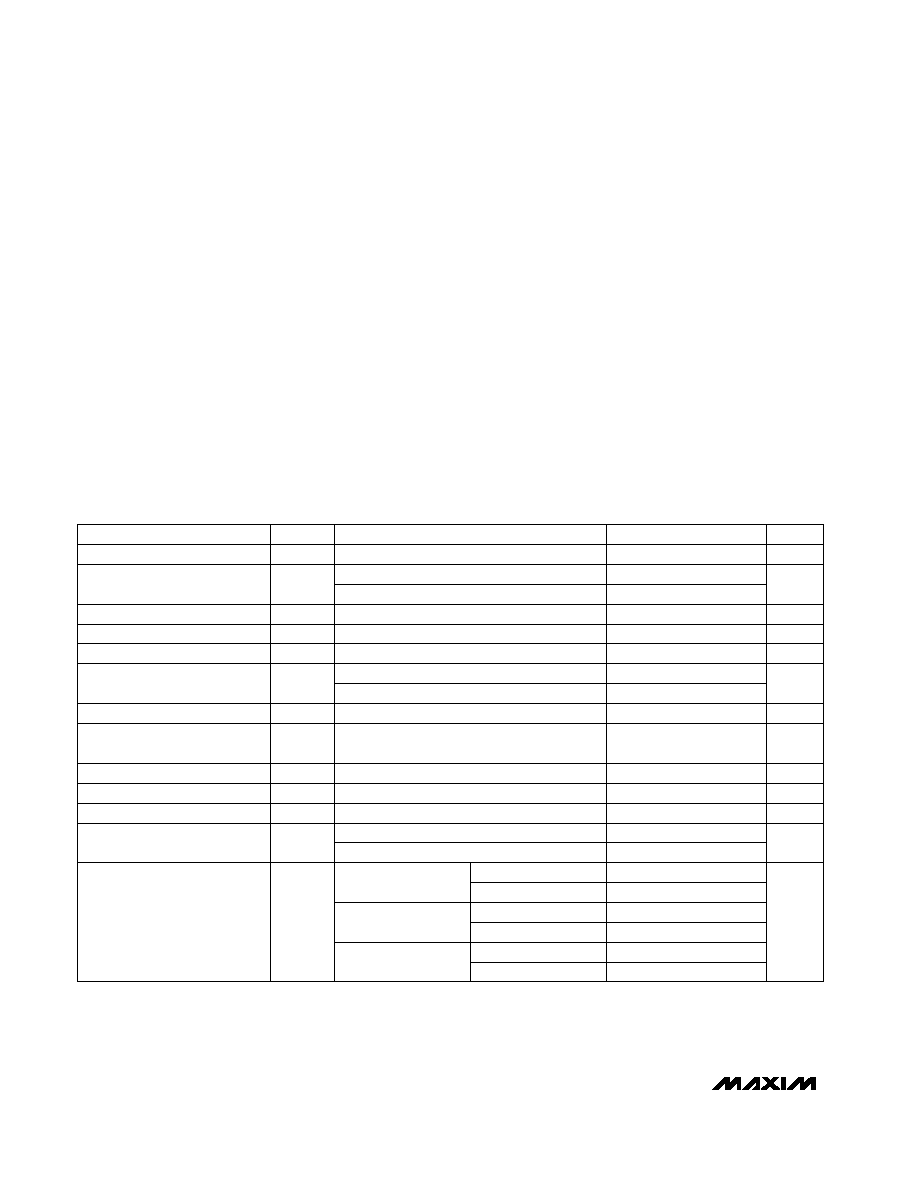
ELECTRICAL CHARACTERISTICS—MAX4074/MAX4075
(VCC = +2.5V to +5.5V, VEE = 0, VIN+ = VIN- = VCC/2, RL =
∞ to VCC/2, TA = TMIN to TMAX, unless otherwise noted. Typical values
are at VCC = +5V and TA = +25°C.) (Note 1)
Stresses beyond those listed under “Absolute Maximum Ratings” may cause permanent damage to the device. These are stress ratings only, and functional
operation of the device at these or any other conditions beyond those indicated in the operational sections of the specifications is not implied. Exposure to
absolute maximum rating conditions for extended periods may affect device reliability.
Supply Voltages (VCC to VEE) ..................................-0.3V to +6V
Voltage Inputs (IN_)
MAX4076/MAX4077/MAX4078 .....(VCC + 0.3V) to (VEE - 0.3V)
MAX4074/MAX4075..........................................................±17V
Output Short-Circuit Duration to Either Supply (OUT_)....Continuous
Continuous Power Dissipation (TA = +70°C)
5-Pin SOT23 (derate 7.1mW/°C above +70°C) ............571mW
14-Pin TSSOP (derate 6.3mW/°C above +70°C) ..........500mW
8-Pin MAX (derate 4.1mW/°C above +70°C) ..............330mW
8-Pin SO (derate 5.88mW/°C above +70°C).................471mW
14-Pin SO (derate 8.33mW/°C above +70°C)...............667mW
Operating Temperature Range ...........................-40°C to +85°C
Junction Temperature ......................................................+150°C
Storage Temperature Range .............................-65°C to +150°C
Lead Temperature (soldering, 10sec) .............................+300°C
Supply Current (per amplifier)
ICC
34
50
A
VCC = 3V
PARAMETER
SYMBOL
MIN
TYP
MAX
UNITS
Inverting Input Resistance
RIN_
80
k
VCC - VOH
300
Input Bias Current (Note 2)
IIN+_
0.8
1000
pA
Input Offset Voltage Drift
0.3
V/°C
Noninverting Input Resistance
RIN_+
1000
M
Negative Input Voltage Range
IN_-
±15
V
Power-Supply Rejection Ratio
PSRR
70
96
dB
Supply Voltage Range
VCC
2.5
5.5
V
300
1000
37
55
Input Offset Voltage
VOS
0.2
3.5
mV
Closed-Loop Output Impedance
ROUT
0.2
VCC - VOH
5
Output Short-Circuit Current
-22
mA
0.5
2.5
VOL - VEE
Output Voltage Swing (Note 4)
100
600
mV
RL = 1k
VCC - VOH
25
150
VOL - VEE
Positive Input Voltage Range
IN_+
11
80
RL = 10k
VOL - VEE
CONDITIONS
AV
≥ +25V/V
Shorted to VCC
AV < +25V/V
Shorted to VEE
VEE -VCC -
0.15
1.2
Guaranteed by functional test (Note 3)
VCC = 2.5V to 5.5V
V
Guaranteed by functional test (Note 3)
0.4
2.5
Guaranteed by PSRR test
VCC = 5V
RL = 1M
RL = 1M
相关PDF资料 |
PDF描述 |
|---|---|
| MAX4133ESD+ | DUAL OP-AMP, 950 uV OFFSET-MAX, 10 MHz BAND WIDTH, PDSO14 |
| MAX4432ESA+ | OP-AMP, 5000 uV OFFSET-MAX, 180 MHz BAND WIDTH, PDSO8 |
| MAX4578EAP+T | 8-CHANNEL, SGL ENDED MULTIPLEXER, PDSO20 |
| MAX4579CAP | High-Voltage, Single 8-to-1/ Dual 4-to-1 Cal-Multiplexers |
| MAX4579CPP | High-Voltage, Single 8-to-1/ Dual 4-to-1 Cal-Multiplexers |
相关代理商/技术参数 |
参数描述 |
|---|---|
| MAX4074ESA | 制造商:MAXIM 制造商全称:Maxim Integrated Products 功能描述:Operational Amplifier |
| MAX4074EUK-T | 制造商:MAXIM 制造商全称:Maxim Integrated Products 功能描述:Operational Amplifier |
| MAX4075 | 制造商:MAXIM 制造商全称:Maxim Integrated Products 功能描述:Micropower, SOT23, Rail-to-Rail, Fixed-Gain, GainAmp/Open-Loop Op Amps |
| MAX4075__ESA | 制造商:MAXIM 制造商全称:Maxim Integrated Products 功能描述:Micropower, SOT23, Rail-to-Rail, Fixed-Gain, GainAmp/Open-Loop Op Amps |
| MAX4075__EUA | 制造商:MAXIM 制造商全称:Maxim Integrated Products 功能描述:Micropower, SOT23, Rail-to-Rail, Fixed-Gain, GainAmp/Open-Loop Op Amps |
发布紧急采购,3分钟左右您将得到回复。