- 您现在的位置:买卖IC网 > PDF目录296461 > MAX4074CAEUK+T (MAXIM INTEGRATED PRODUCTS INC) OP-AMP, 3500 uV OFFSET-MAX, 4 MHz BAND WIDTH, PDSO5 PDF资料下载
参数资料
| 型号: | MAX4074CAEUK+T |
| 厂商: | MAXIM INTEGRATED PRODUCTS INC |
| 元件分类: | 运算放大器 |
| 英文描述: | OP-AMP, 3500 uV OFFSET-MAX, 4 MHz BAND WIDTH, PDSO5 |
| 封装: | SOT-23, 5 PIN |
| 文件页数: | 4/20页 |
| 文件大小: | 649K |
| 代理商: | MAX4074CAEUK+T |
MAX4074–MAX4078
Micropower, SOT23, Rail-to-Rail,
Fixed-Gain, GainAmp/Open-Loop Op Amps
12
______________________________________________________________________________________
GainAmp Signal Coupling
and Configurations
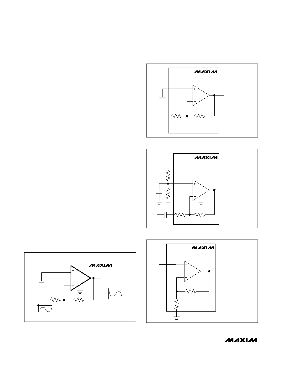
Common op amp configurations include both noninvert-
ing and inverting amplifiers. Figures 3–6 show various
single- and dual-supply circuit configurations. In single-
supply systems, use a resistor-divider to bias the nonin-
verting input. A lowpass filter capacitor from the op amp
input to ground (Figure 5) prevents high-frequency
power-supply noise from coupling into the op amp input.
Dual-supply systems can have ground-referenced sig-
nals DC-coupled into the inverting or noninverting inputs.
Supply Bypassing and Board Layout
All devices in this GainAmp family operate from a +2.5V
to +5.5V single supply or from ±1.25V to ±2.75V dual
supplies. For single-supply operation, bypass the power
supply with a 0.1F capacitor to ground. For dual sup-
plies, bypass each supply to ground. Bypass with
capacitors as close to the device as possible to mini-
mize lead inductance and noise. A printed circuit board
with a low-inductance ground plane is recommended.
Capacitive-Load Stability
Driving large capacitive loads can cause instability in
most low-power, rail-to-rail output amplifiers. The fixed-
gain amplifiers of this GainAmp family are stable with
capacitive loads up to 100pF. Stability with higher
capacitive loads can be improved by adding an isola-
tion resistor in series with the op amp output, as shown
in Figure 7. This resistor improves the circuit’s phase
margin by isolating the load capacitor from the amplifi-
er’s output. In Figure 8, a 220pF capacitor is driven with
a 100
isolation resistor exhibiting some overshoot but
no oscillation. Figures 9 and 10 show the typical small-
signal pulse responses of GainAmp fixed-gain ampli-
fiers with 47pF and 100pF capacitive loads and no
isolation resistor
MAX4074
VCC
RG
RF
VIN
VOUT =
-RF
(VIN)
RG
Figure 3. Single-Supply, DC-Coupled Inverting Amplifier with
Negative Input Voltage
MAX4074
VEE
VCC
RG
RF
VIN
VOUT = - VIN
(
RF )
RG
Figure 4. Dual-Supply, DC-Coupled Inverting Amplifier
MAX4074
VCC
RG
RF
VIN
0.1
F
VOUT =
VCC
- VIN
(
RF )
2
RG
Figure 5. Single-Supply, AC-Coupled Inverting Amplifier
MAX4074
VEE
VCC
RG
RF
VIN
VOUT = VIN
(1+
RF )
RG
Figure 6. Dual-Supply, DC-Coupled Noninverting Amplifier
相关PDF资料 |
PDF描述 |
|---|---|
| MAX4133ESD+ | DUAL OP-AMP, 950 uV OFFSET-MAX, 10 MHz BAND WIDTH, PDSO14 |
| MAX4432ESA+ | OP-AMP, 5000 uV OFFSET-MAX, 180 MHz BAND WIDTH, PDSO8 |
| MAX4578EAP+T | 8-CHANNEL, SGL ENDED MULTIPLEXER, PDSO20 |
| MAX4579CAP | High-Voltage, Single 8-to-1/ Dual 4-to-1 Cal-Multiplexers |
| MAX4579CPP | High-Voltage, Single 8-to-1/ Dual 4-to-1 Cal-Multiplexers |
相关代理商/技术参数 |
参数描述 |
|---|---|
| MAX4074ESA | 制造商:MAXIM 制造商全称:Maxim Integrated Products 功能描述:Operational Amplifier |
| MAX4074EUK-T | 制造商:MAXIM 制造商全称:Maxim Integrated Products 功能描述:Operational Amplifier |
| MAX4075 | 制造商:MAXIM 制造商全称:Maxim Integrated Products 功能描述:Micropower, SOT23, Rail-to-Rail, Fixed-Gain, GainAmp/Open-Loop Op Amps |
| MAX4075__ESA | 制造商:MAXIM 制造商全称:Maxim Integrated Products 功能描述:Micropower, SOT23, Rail-to-Rail, Fixed-Gain, GainAmp/Open-Loop Op Amps |
| MAX4075__EUA | 制造商:MAXIM 制造商全称:Maxim Integrated Products 功能描述:Micropower, SOT23, Rail-to-Rail, Fixed-Gain, GainAmp/Open-Loop Op Amps |
发布紧急采购,3分钟左右您将得到回复。