- 您现在的位置:买卖IC网 > PDF目录1941 > MAX459CQH-D (Maxim Integrated Products)IC VIDEO CROSSPOINT SWIT 44PLCC PDF资料下载
参数资料
| 型号: | MAX459CQH-D |
| 厂商: | Maxim Integrated Products |
| 文件页数: | 11/17页 |
| 文件大小: | 0K |
| 描述: | IC VIDEO CROSSPOINT SWIT 44PLCC |
| 产品培训模块: | Lead (SnPb) Finish for COTS Obsolescence Mitigation Program |
| 标准包装: | 28 |
| 功能: | 视频交叉点开关 |
| 电路: | 1 x 8:4 |
| 工作温度: | 0°C ~ 70°C |
| 安装类型: | 表面贴装 |
| 封装/外壳: | 44-LCC(J 形引线) |
| 供应商设备封装: | 44-PLCC(16.59x16.59) |
| 包装: | 管件 |
MAX458/MAX459
8x4 Video Crosspoint Switches with Buffers
2
_______________________________________________________________________________________
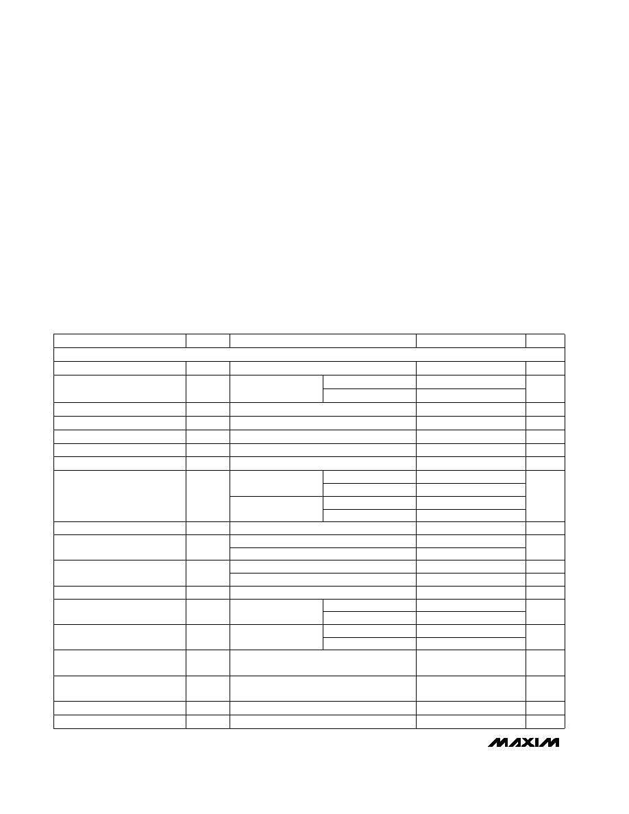
ABSOLUTE MAXIMUM RATINGS
ELECTRICAL CHARACTERISTICS
(VCC = +5V, VEE = -5V, -2V
≤ VIN ≤ +2V, output load resistor (RL) = 150, TA = TMIN to TMAX, unless otherwise noted.
Typical values are at TA = +25°C.)
Stresses beyond those listed under “Absolute Maximum Ratings” may cause permanent damage to the device. These are stress ratings only, and functional
operation of the device at these or any other conditions beyond those indicated in the operational sections of the specifications is not implied. Exposure to
absolute maximum rating conditions for extended periods may affect device reliability.
Total Supply Voltage (VCC to VEE) .........................................12V
Positive Supply Voltage (VCC to GND).....................................6V
Negative Supply Voltage (VEE to GND) ...................................6V
Analog Input/Output Voltage ...........(VCC + 0.3V) to (VEE - 0.3V)
Digital Input Voltage ...................................(VCC + 0.3V) to -0.3V
Duration of Output Short Circuit to GND (Note 1) ......Continuous
Continuous Power Dissipation
Plastic DIP (derate 17mW/°C above +70°C) ..............1333mW
PLCC (derate 13mW/°C above +70°C) ......................1067mW
Operating Temperature Ranges
MAX45_C_ _ ........................................................0°C to +70°C
MAX45_E_ _......................................................-40°C to +85°C
Junction Temperature ......................................................+150°C
Storage Temperature Range .............................-65°C to +160°C
Lead Temperature (soldering, 10sec) .............................+300°C
(Note 5)
Any channel
VIN = 0V,
all amplifiers enabled
MAX458 (Note 3)
VIN = 0V (Note 2)
VIN = 0V, input programmed to one output
Input programmed to one output
VIN = 10MHz sine wave
Input channel on or off
VIN = 1kHz sine wave
CONDITIONS
V
0.8
VIL
Logic Input Low Voltage
V
2.0
VIH
Logic Input High Voltage
mA
15
26
Positive Supply Current in
Shutdown
50
100
mA
60
75
85
ICC
Positive Power-Supply Current
pF
12
COUT
Disabled Output Capacitance
4.0
0.05
ROUT
Enabled Output Resistance
20
mV
515
VOS
Input Offset Voltage
V
±2
±3
VOUT
Output Voltage Swing
1.0
0.1
0.5
mV
310
VOS
Input Offset Voltage Match
A
±1
±5
IIN
On Input Bias Current
M
0.50
5.0
RIN
On Input Resistance
pF
7
CIN
Input Capacitance
UNITS
MIN
TYP
MAX
SYMBOL
PARAMETER
Note 1: Outputs may be shorted to any supply pin or ground as long as package power dissipation ratings are not exceeded.
TA = +25°C
TA = TMIN to TMAX
TA = +25°C
TA = TMIN to TMAX
TA = +25°C
MAX459 (Note 4)
TA = TMIN to TMAX
2.0
%
0.1
1.0
DC Voltage Gain Accuracy
MAX459
MAX458
0.70
1.0
M
0.25
1.0
ROUT
Disabled Output Resistance
TA = +25°C
TA = TMIN to TMAX
VIN = 0V,
all amplifiers enabled
40
90
TA = +25°C
TA = TMIN to TMAX
mA
50
65
75
IEE
Negative Power-Supply Current
mA
712
Negative Supply Current in
Shutdown
k
V
-2
+2
Input Voltage Range
VS = ±4.75V to ±5.25V
dB
50
60
PSRR
Power-Supply Rejection Ratio
STATIC SPECIFICATIONS
相关PDF资料 |
PDF描述 |
|---|---|
| MAX4603EAE | IC SWITCH QUAD SPST 16SSOP |
| MAX4604CPE | IC SWITCH QUAD SPST 16DIP |
| MAX4609CPE | IC SWITCH DUAL SPST 16DIP |
| MAX4612CSD | IC SWITCH QUAD SPST 14SOIC |
| MAX4613CUE | IC SWITCH QUAD SPST 16TSSOP |
相关代理商/技术参数 |
参数描述 |
|---|---|
| MAX459CQH-DW | 功能描述:模拟和数字交叉点 IC RoHS:否 制造商:Micrel 配置:2 x 2 封装 / 箱体:MLF-16 数据速率:10.7 Gbps 输入电平:CML, LVDS, LVPECL 输出电平:CML 电源电压-最大:3.6 V 电源电压-最小:2.375 V 最大工作温度:+ 85 C 最小工作温度:- 40 C 产品:Digital Crosspoint 封装:Tube |
| MAX459CQH-DW-T | 功能描述:模拟和数字交叉点 IC RoHS:否 制造商:Micrel 配置:2 x 2 封装 / 箱体:MLF-16 数据速率:10.7 Gbps 输入电平:CML, LVDS, LVPECL 输出电平:CML 电源电压-最大:3.6 V 电源电压-最小:2.375 V 最大工作温度:+ 85 C 最小工作温度:- 40 C 产品:Digital Crosspoint 封装:Tube |
| MAX459CQH-TD | 功能描述:视频开关 IC RoHS:否 制造商:Texas Instruments 开关数量:4 开启电阻(最大值):12 Ohms 传播延迟时间: 开启时间(最大值): 关闭时间(最大值): 最大工作温度:+ 85 C 最小工作温度:- 40 C 封装 / 箱体:WQFN-42 封装:Reel |
| MAX459EPL | 功能描述:视频开关 IC RoHS:否 制造商:Texas Instruments 开关数量:4 开启电阻(最大值):12 Ohms 传播延迟时间: 开启时间(最大值): 关闭时间(最大值): 最大工作温度:+ 85 C 最小工作温度:- 40 C 封装 / 箱体:WQFN-42 封装:Reel |
| MAX459EVKIT-PLC | 制造商:Rochester Electronics LLC 功能描述: 制造商:Maxim Integrated Products 功能描述: |
发布紧急采购,3分钟左右您将得到回复。