- 您现在的位置:买卖IC网 > PDF目录16545 > MAX4807CTN+T (Maxim Integrated Products)IC DGTL PULSER DUAL 56TQFN PDF资料下载
参数资料
| 型号: | MAX4807CTN+T |
| 厂商: | Maxim Integrated Products |
| 文件页数: | 9/20页 |
| 文件大小: | 0K |
| 描述: | IC DGTL PULSER DUAL 56TQFN |
| 产品培训模块: | Lead (SnPb) Finish for COTS Obsolescence Mitigation Program |
| 标准包装: | 2,500 |
| 应用: | 通用型,过电压保护 |
| 电流 - 电源: | 100µA |
| 电源电压: | 2.7 V ~ 6 V |
| 工作温度: | 0°C ~ 70°C |
| 安装类型: | 表面贴装 |
| 封装/外壳: | 56-WFQFN 裸露焊盘 |
| 供应商设备封装: | 56-TQFN-EP(7x7) |
| 包装: | 带卷 (TR) |
�� �
�
�Dual,� Unipolar/Bipolar,� High-Voltage�
�Digital� Pulsers�
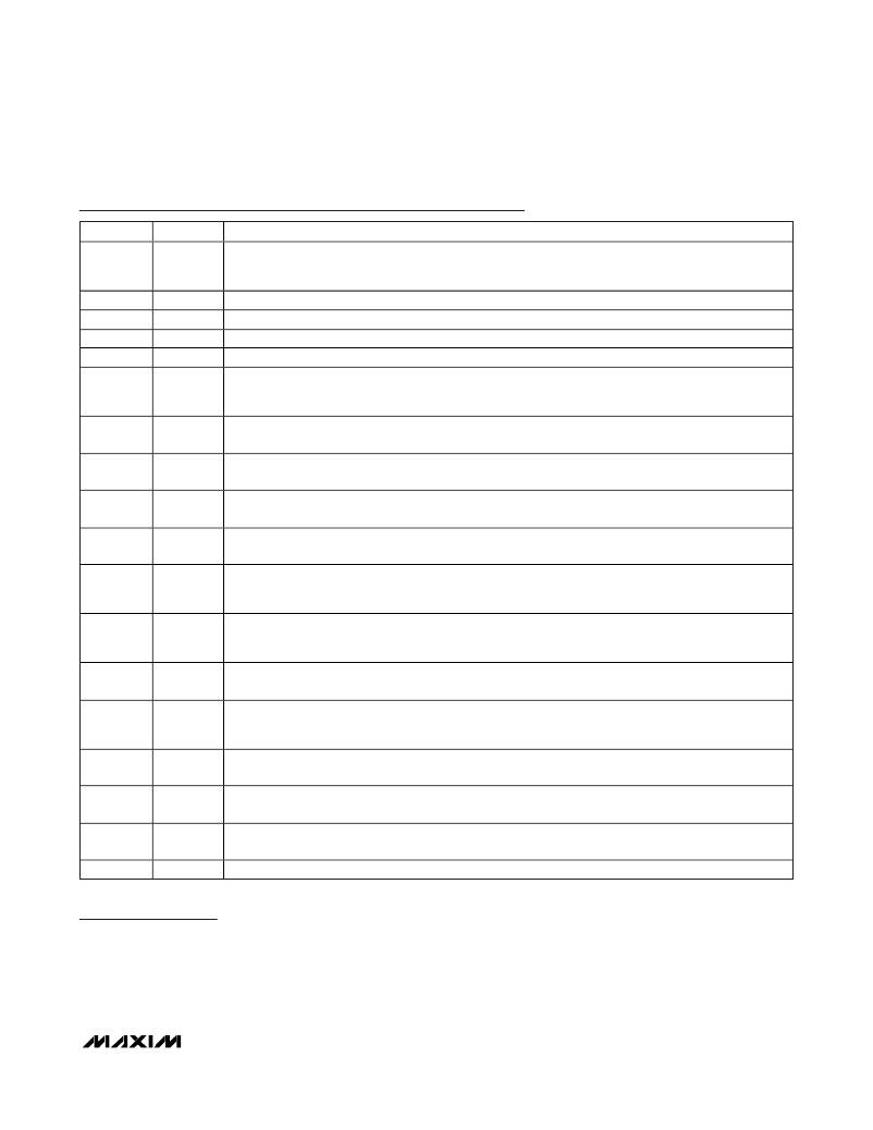
�Pin� Description� (continued)�
�PIN�
�31,� 32�
�34�
�35�
�37�
�38�
�40,� 41�
�42�
�43�
�46�
�47�
�48�
�49�
�50�
�51�
�52�
�53�
�56�
�—�
�NAME�
�V� NN2�
�ON2�
�OCN2�
�OCP2�
�OP2�
�V� PP2�
�C� GP2�
�C� DP2�
�C� GC2�
�C� DC2�
�V� EE2�
�V� DD�
�V� SS�
�V� EE1�
�C� DC1�
�C� GC1�
�C� DP1�
�EP�
�FUNCTION�
�Channel� 2� High-Side� Negative� Supply� Voltage� Input.� Bypass� V� NN2� to� GND� with� a� 0.1μF� capacitor� as�
�close� as� possible� to� the� device.� (See� Power� Supplies� and� Bypassing� in� the� Applications� Information�
�section.)� Depending� on� the� application,� additional� bypassing� may� be� required.�
�Channel� 2� Low-Side� Drain� Output�
�Channel� 2� Low-Side� Clamp� Output�
�Channel� 2� High-Side� Clamp� Output�
�Channel� 2� High-Side� Drain� Output�
�Channel� 2� High-Side� Positive� Supply� Voltage� Input.� Bypass� V� PP2� to� GND� with� a� 0.1μF� capacitor� as� close�
�as� possible� to� the� device.� (See� Power� Supplies� and� Bypassing� in� the� Applications� Information� section.)�
�Depending� on� the� application,� additional� bypassing� may� be� required.�
�Channel� 2� High-Side� Gate� Input.� Connect� a� 1nF� to� 10nF� capacitor� between� C� DP2� and� C� GP2� as� close� as�
�possible� to� the� device.�
�Channel� 2� High-Side� Driver� Output.� Connect� a� 1nF� to� 10nF� capacitor� between� C� DP2� and� C� GP2� as� close�
�as� possible� to� the� device.�
�Channel� 2� High-Side� Clamp� Gate� Input.� Connect� a� 1nF� to� 10nF� capacitor� between� C� DC2� and� C� GC2� as�
�close� as� possible� to� the� device.�
�Channel� 2� High-Side� Clamp� Driver� Output.� Connect� a� 1nF� to� 10nF� capacitor� between� C� DC2� and� C� GC2� as�
�close� as� possible� to� the� device.�
�Channel� 2� Negative� Supply� Input.� Gate-drive� supply� voltage� for� the� OCP2� clamp.� Bypass� V� EE2� to� GND�
�with� a� 0.1μF� capacitor� as� close� as� possible� to� the� device.� (See� Power� Supplies� and� Bypassing� in� the�
�Applications� Information� section.)� Depending� on� the� application,� additional� bypassing� may� be� required.�
�Logic� Supply� Voltage� Input.� Bypass� V� DD� to� GND� with� a� 0.1μF� capacitor� as� close� as� possible� to� the�
�device.� (See� Power� Supplies� and� Bypassing� in� the� Applications� Information� section.)� Depending� on� the�
�application,� additional� bypassing� may� be� required.�
�Substrate� Voltage.� Connect� V� SS� to� a� voltage� equal� to� or� more� negative� than� the� more� negative� of� V� NN1� or�
�V� NN2� .�
�Channel� 1� Negative� Supply� Input.� Gate-drive� supply� voltage� for� the� OCP1� clamp.� Bypass� V� EE1� to� GND�
�with� a� 0.1μF� capacitor� as� close� as� possible� to� the� device.� (See� Power� Supplies� and� Bypassing� in� the�
�Applications� Information� section.)� Depending� on� the� application,� additional� bypassing� may� be� required.�
�Channel� 1� High-Side� Clamp� Driver� Output.� Connect� a� 1nF� to� 10nF� capacitor� between� C� DC1� and� C� GC1� as�
�close� as� possible� to� the� device.�
�Channel� 1� High-Side� Clamp� Gate� Input.� Connect� a� 1nF� to� 10nF� capacitor� between� C� DC1� and� C� GC1� as�
�close� as� possible� to� the� device.�
�Channel� 1� High-Side� Driver� Output.� Connect� a� 1nF� to� 10nF� capacitor� between� C� DP1� and� C� GP1� as� close�
�as� possible� to� the� device.�
�Exposed� Pad.� EP� must� be� connected� to� V� SS� .� Do� not� use� EP� as� the� only� V� SS� connection� for� the� device.�
�Detailed� Description�
�The� MAX4806/MAX4807/MAX4808� are� dual� high-volt-�
�age,� high-speed� pulsers� that� can� be� independently� con-�
�figured� for� either� unipolar� or� bipolar� pulse� outputs.� These�
�devices� have� independent� logic� inputs� for� full� pulse� con-�
�trol� and� independent� active� clamps.� The� clamp� input,�
�INC_,� can� be� set� high� to� activate� the� clamp� automatical-�
�ly� when� the� device� is� not� pulsing� to� the� positive� or� nega-�
�tive� high-voltage� supplies.� (See� Figures� 1,� 2,� and� 3.)�
�Logic� Inputs� (INP_,� INN_,� INC_,� EN_,� SHDN� )�
�The� MAX4806/MAX4807/MAX4808� have� a� total� of� nine�
�logic� input� signals.� SHDN� controls� power-up� and� -down�
�of� the� device.� There� are� two� sets� of� INP_,� INN_,� INC_�
�and� EN_� signals:� one� for� each� channel.� INP_� controls� the�
�_______________________________________________________________________________________�
�9�
�相关PDF资料 |
PDF描述 |
|---|---|
| PX0840/B/3M00 | CABLE PLUG IP68 USB B-A 3M |
| MAX5042ATN+T | IC PWR W/MOSFET HS 56-TQFN |
| PX0441/2M00 | CABLE IP68 MINI B TO A USB 2M |
| BA6219BFP-YE2 | IC DRIVER MOTOR REVERSE HSOP25 |
| VI-J5Y-EZ-S | CONVERTER MOD DC/DC 3.3V 16.5W |
相关代理商/技术参数 |
参数描述 |
|---|---|
| MAX480C/D | 功能描述:运算放大器 - 运放 RoHS:否 制造商:STMicroelectronics 通道数量:4 共模抑制比(最小值):63 dB 输入补偿电压:1 mV 输入偏流(最大值):10 pA 工作电源电压:2.7 V to 5.5 V 安装风格:SMD/SMT 封装 / 箱体:QFN-16 转换速度:0.89 V/us 关闭:No 输出电流:55 mA 最大工作温度:+ 125 C 封装:Reel |
| MAX480CPA | 功能描述:运算放大器 - 运放 RoHS:否 制造商:STMicroelectronics 通道数量:4 共模抑制比(最小值):63 dB 输入补偿电压:1 mV 输入偏流(最大值):10 pA 工作电源电压:2.7 V to 5.5 V 安装风格:SMD/SMT 封装 / 箱体:QFN-16 转换速度:0.89 V/us 关闭:No 输出电流:55 mA 最大工作温度:+ 125 C 封装:Reel |
| MAX480CSA | 功能描述:运算放大器 - 运放 RoHS:否 制造商:STMicroelectronics 通道数量:4 共模抑制比(最小值):63 dB 输入补偿电压:1 mV 输入偏流(最大值):10 pA 工作电源电压:2.7 V to 5.5 V 安装风格:SMD/SMT 封装 / 箱体:QFN-16 转换速度:0.89 V/us 关闭:No 输出电流:55 mA 最大工作温度:+ 125 C 封装:Reel |
| MAX480CSA+ | 功能描述:运算放大器 - 运放 RoHS:否 制造商:STMicroelectronics 通道数量:4 共模抑制比(最小值):63 dB 输入补偿电压:1 mV 输入偏流(最大值):10 pA 工作电源电压:2.7 V to 5.5 V 安装风格:SMD/SMT 封装 / 箱体:QFN-16 转换速度:0.89 V/us 关闭:No 输出电流:55 mA 最大工作温度:+ 125 C 封装:Reel |
| MAX480CSA+T | 功能描述:运算放大器 - 运放 RoHS:否 制造商:STMicroelectronics 通道数量:4 共模抑制比(最小值):63 dB 输入补偿电压:1 mV 输入偏流(最大值):10 pA 工作电源电压:2.7 V to 5.5 V 安装风格:SMD/SMT 封装 / 箱体:QFN-16 转换速度:0.89 V/us 关闭:No 输出电流:55 mA 最大工作温度:+ 125 C 封装:Reel |
发布紧急采购,3分钟左右您将得到回复。