- 您现在的位置:买卖IC网 > PDF目录15152 > MAX5003CSE+T (Maxim Integrated Products)IC REG CTRLR FLYBK ISO VM 16SOIC PDF资料下载
参数资料
| 型号: | MAX5003CSE+T |
| 厂商: | Maxim Integrated Products |
| 文件页数: | 14/16页 |
| 文件大小: | 0K |
| 描述: | IC REG CTRLR FLYBK ISO VM 16SOIC |
| 产品培训模块: | Lead (SnPb) Finish for COTS Obsolescence Mitigation Program |
| 标准包装: | 2,500 |
| PWM 型: | 电压模式 |
| 输出数: | 1 |
| 频率 - 最大: | 1.2MHz |
| 占空比: | 75% |
| 电源电压: | 11 V ~ 110 V |
| 降压: | 无 |
| 升压: | 无 |
| 回扫: | 是 |
| 反相: | 无 |
| 倍增器: | 无 |
| 除法器: | 无 |
| Cuk: | 无 |
| 隔离: | 是 |
| 工作温度: | 0°C ~ 70°C |
| 封装/外壳: | 16-SOIC(0.154",3.90mm 宽) |
| 包装: | 带卷 (TR) |
�� �
�
�High-Voltage� PWM�
�Power-Supply� Controller�
�where:�
�R� MAXTON� =� Resistor� between� the� MAXTON� pin� and�
�ground�
�V� MIN� =� Minimum� power-line� voltage�
�V� UVL� =� Power-line� trip� voltage�
�DC� MAX� (V� MIN� )� =� Maximum� duty� cycle� at� minimum�
�the� ripple� will� be� a� fraction� of� this� depending� on� the�
�duty� cycle.� For� a� 50%� duty� cycle,� the� ripple� due� to�
�the� capacitance� is� approximately� 45mV.�
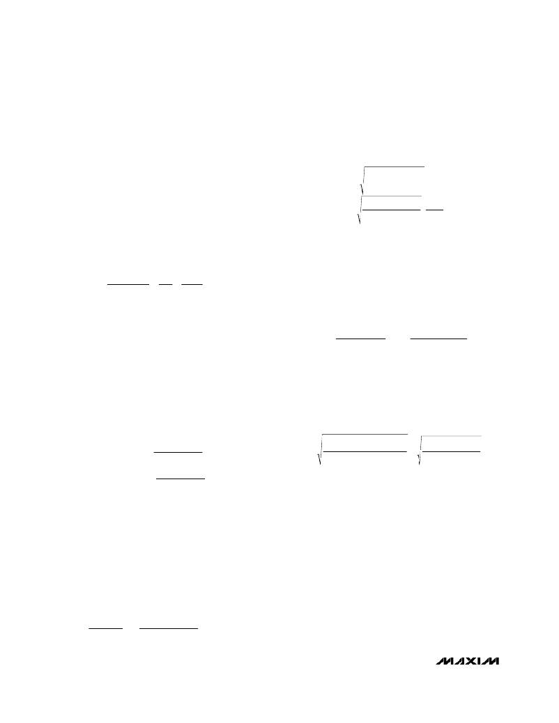
�8)The� PWM� gain� can� be� calculated� from:�
�dV� OUT� R� L� ?� V� MIN� ?�
�A� PWM� =� =� ?� ?� DC� MAX� (� VMI�
�dV� CON� 2� ×� L� PRI� ×?� SW� ?� 2.0V� ?�
�?� ?� 50� %� ?� 3�
�power-line voltage�
�For� this� application� circuit,� a� 10%� margin� is� reason-�
�able,� so� the� value� used� is� 50k� ?� .� This� gives� a� maxi-�
�=�
�R� L� ?� 36� V� ?�
�2� � L� PRI� � ?� SW� ?� 2� .� 0� V� ?�
�DC(V� CON,VIN� )� =� ?� CON�
�?� ?� ?� ?� ?� � DC� MAX(VMIN)�
�≈� ?� ?� ?� ?� ?� ?� 50%�
�?� P� =� ?� ?� =� ?� ?�
�mum duty cycle of 50%. The maximum duty cycle�
�can� now� be� expressed� as:�
�?� V� -� 0.5V� ?� ?� V� MIN� ?� ?� ?� SW� ?�
�?� 2.0V� ?� ?� V� IN� ?� ?� ?� NOM� ?�
�?� V� CON� -� 0.5V� ?� ?� 36V� ?� ?� ?� SW� ?�
�?� 2.0V� ?� ?� V� IN� ?� ?� ?� NOM� ?�
�where:�
�V� CON� =� Voltage� at� the� CON� pin,� input� of� the� PWM�
�comparator�
�DC(V� CON� ,� V� IN� )� =� Duty� cycle,� function� of� V� CON� and�
�V� IN�
�0.5V� and� 2.5V� are� the� values� at� the� beginning� and�
�end� of� the� PWM� ramp.�
�The� term� ?� SW� /� ?� NOM� varies� from� 0.8� to� 1.2� to� allow�
�for� clock� frequency� variation.� If� the� clock� is� running�
�at� 300kHz� and� the� input� voltage� is� fixed,� then� the�
�duty� cycle� is� a� scaled� portion� of� the� maximum� duty�
�cycle,� determined� by� V� CON� .�
�Note� that� while� the� above� formula� incorporates� the�
�product� of� the� maximum� duty� cycle� and� V� IN� ,� it� is�
�independent� of� V� IN� .� For� 1A� output� (R� L� =� 5� ?� ),� the�
�PWM� gain� is� +3.0V/V.� For� a� 10%� load� (R� L� =� 50� ?� ),�
�the� gain� is� multiplied� by� the� square� root� of� 10� and�
�becomes� +10V/V.� The� pole� of� the� system� due� to� the�
�output� filter� is� 1� /� 2� π� RC,� where� R� is� the� load� resis-�
�tance� and� C� the� filter� capacitor.� Choosing� a� capaci-�
�tor� and� calculating� the� pole� frequency� by:�
�?� 1� ?� ?� 1� ?�
�?� 2� π� ×� R� L� ×� C� L� ?� ?� 2� π� ×� 5� ?� ×� 44� μ� F� ?�
�it� is� 723Hz� at� full� load.� At� 10%� load� it� will� be� 72Hz,�
�since� the� load� resistor� is� then� 50� ?� instead� of� 5� ?� .� The�
�total� loop� gain� is� equal� to� the� PWM� gain� times� the�
�gain� in� the� combination� of� the� voltage� divider� and�
�the� error� amplifier.� The� worst� case� for� phase� margin�
�is� at� full� load.� For� a� phase� margin� of� 60� degrees,� this�
�midband� gain� (G)� must� be� set� to� be� less� than:�
�DC(V� CON� ,V� MIN� )� =� ?� CON�
�?� V� -� 0.5V� ?�
�?� 50%�
�?� 2.0V� ?�
�G� <�
�?� UErrorAmp�
�tan(� PM� )� ×� A� PWM� ×?� P�
�=�
�1� MHz�
�1� .� 7� � 3� � 723� Hz�
�DC(V� CON� MAX� )� =� ?� CON�
�?� 25%�
�?� V� -� 0.5V� ?�
�,V�
�?� 2.0V� ?�
�DC(2.5V,V� MIN� )� =� 50%�
�DC(2.5V,V� MAX� )� =� 25%�
�DC(0.5V,V� MIN� )� =� 0�
�DC(0.5V,V� MAX� )� =� 0�
�7)� Low-ESR/ESL� ceramic� capacitors� were� used� in� this�
�application.� The� output� filter� is� made� by� two� 22μF�
�ceramic� capacitors� in� parallel.� Normally,� the� ESR� of�
�a� capacitor� is� a� dominant� factor� determining� the� rip-�
�ple,� but� in� this� case� it� is� the� capacitor� value.�
�Calculating�
�where:�
�?� U� =� Unity-gain� frequency� of� error� amplifier�
�PM� =� Phase� margin� angle�
�The� DC� accuracy� of� the� regulator� is� a� function� of� the�
�DC� gain.� For� 1%� accuracy,� a� DC� gain� of� 20� is� required.�
�Since� the� maximum� midband� gain� for� a� stable�
�response� is� 16,� an� integrator� with� a� flat� midband� gain�
�given� by� a� zero� is� used.� The� midband� gain� is� less� than�
�16,� to� preserve� stability,� and� the� DC� gain� is� much� larger�
�than� 20,� to� achieve� high� DC� accuracy.�
�Optimization� on� the� bench� showed� that� a� midband� gain�
�of� 5� gave� fast� transient� response� and� settling� with� no�
�ringing.� The� zero� was� pushed� as� high� in� frequency� as�
�I� OUT�
�?� SW� � C�
�=�
�1� A�
�300� kHz� ×� 44� μ� F�
�=� 76� mV�
�possible� without� losing� stability.� The� zero� must� be� a�
�factor� of� two� or� so� below� the� system� unity-gain� frequen-�
�cy� (crossover� frequency)� at� minimum� load.� With� the�
�14�
�______________________________________________________________________________________�
�相关PDF资料 |
PDF描述 |
|---|---|
| VE-JTJ-EY-F4 | CONVERTER MOD DC/DC 36V 50W |
| MAX5003CEE+T | IC REG CTRLR FLYBK ISO VM 16QSOP |
| MAX5003ESE+T | IC REG CTRLR FLYBK ISO VM 16SOIC |
| MAX15004AAUE+T | IC REG CTRLR PWM CM 16-TSSOP |
| EBM36DCTI-S288 | CONN EDGECARD 72POS .156 EXTEND |
相关代理商/技术参数 |
参数描述 |
|---|---|
| MAX5003EEE | 功能描述:电压模式 PWM 控制器 PWM Power-Supply Controller RoHS:否 制造商:Texas Instruments 输出端数量:1 拓扑结构:Buck 输出电压:34 V 输出电流: 开关频率: 工作电源电压:4.5 V to 5.5 V 电源电流:600 uA 最大工作温度:+ 125 C 最小工作温度:- 40 C 封装 / 箱体:WSON-8 封装:Reel |
| MAX5003EEE+ | 功能描述:电压模式 PWM 控制器 PWM Power-Supply Controller RoHS:否 制造商:Texas Instruments 输出端数量:1 拓扑结构:Buck 输出电压:34 V 输出电流: 开关频率: 工作电源电压:4.5 V to 5.5 V 电源电流:600 uA 最大工作温度:+ 125 C 最小工作温度:- 40 C 封装 / 箱体:WSON-8 封装:Reel |
| MAX5003EEE+G39 | 制造商:Rochester Electronics LLC 功能描述: 制造商:Maxim Integrated Products 功能描述: |
| MAX5003EEE+T | 功能描述:电压模式 PWM 控制器 PWM Power-Supply Controller RoHS:否 制造商:Texas Instruments 输出端数量:1 拓扑结构:Buck 输出电压:34 V 输出电流: 开关频率: 工作电源电压:4.5 V to 5.5 V 电源电流:600 uA 最大工作温度:+ 125 C 最小工作温度:- 40 C 封装 / 箱体:WSON-8 封装:Reel |
| MAX5003EEE-T | 功能描述:电压模式 PWM 控制器 PWM Power-Supply Controller RoHS:否 制造商:Texas Instruments 输出端数量:1 拓扑结构:Buck 输出电压:34 V 输出电流: 开关频率: 工作电源电压:4.5 V to 5.5 V 电源电流:600 uA 最大工作温度:+ 125 C 最小工作温度:- 40 C 封装 / 箱体:WSON-8 封装:Reel |
发布紧急采购,3分钟左右您将得到回复。