- 您现在的位置:买卖IC网 > PDF目录1842 > MAX5060ATI+ (Maxim Integrated Products)IC REG CTRLR BUCK PWM CM 28-TQFN PDF资料下载
参数资料
| 型号: | MAX5060ATI+ |
| 厂商: | Maxim Integrated Products |
| 文件页数: | 20/31页 |
| 文件大小: | 0K |
| 描述: | IC REG CTRLR BUCK PWM CM 28-TQFN |
| 产品培训模块: | Lead (SnPb) Finish for COTS Obsolescence Mitigation Program |
| 标准包装: | 60 |
| PWM 型: | 电流模式 |
| 输出数: | 1 |
| 频率 - 最大: | 1.5MHz |
| 占空比: | 90% |
| 电源电压: | 4.75 V ~ 28 V |
| 降压: | 是 |
| 升压: | 无 |
| 回扫: | 无 |
| 反相: | 无 |
| 倍增器: | 无 |
| 除法器: | 无 |
| Cuk: | 无 |
| 隔离: | 无 |
| 工作温度: | -40°C ~ 125°C |
| 封装/外壳: | 28-WFQFN 裸露焊盘 |
| 包装: | 管件 |
第1页第2页第3页第4页第5页第6页第7页第8页第9页第10页第11页第12页第13页第14页第15页第16页第17页第18页第19页当前第20页第21页第22页第23页第24页第25页第26页第27页第28页第29页第30页第31页
�� �
�
�0.6V� to� 5.5V� Output,� Parallelable,�
�Average-Current-Mode� DC-DC� Controllers�
�where� ?� I� L� =� peak-to-peak� inductor� current.� Choose�
�RC2� =� 10� ?� ,� V� CC� =� 5.1V,� and� R� SENSE� is� a� current-�
�sense� resistor.� Note� that� the� current� limit� of� MAX5061� is�
�V� OUT� (� NL� )� =� [(� REF� +� REF�
�)� � R� H� ]� +� V� REF�
�reduced� by� 3mV� /� R� SENSE� .�
�The� no-load� output� voltage� depends� on� the� R� H� ,� R� F� ,�
�V� REF� (0.6V)� and� the� fixed� DC� bias� voltage� at� CSP� -�
�CSN.� The� following� equation� assumes� a� 3mV� bias� volt-�
�age� at� CSP� -� CSN.�
�V� V� ?� 0� .� 1�
�R� L� R� F�
�Adaptive� Voltage� Positioning�
�V� CNTR� +�
�?� V� OUT� /2�
�V� CNTR�
�V� CNTR� -�
�?� V� OUT� /2�
�Powering� new-generation� processors� requires� new�
�techniques� to� reduce� cost,� size,� and� power� dissipation.�
�Voltage� positioning� reduces� the� total� number� of� output�
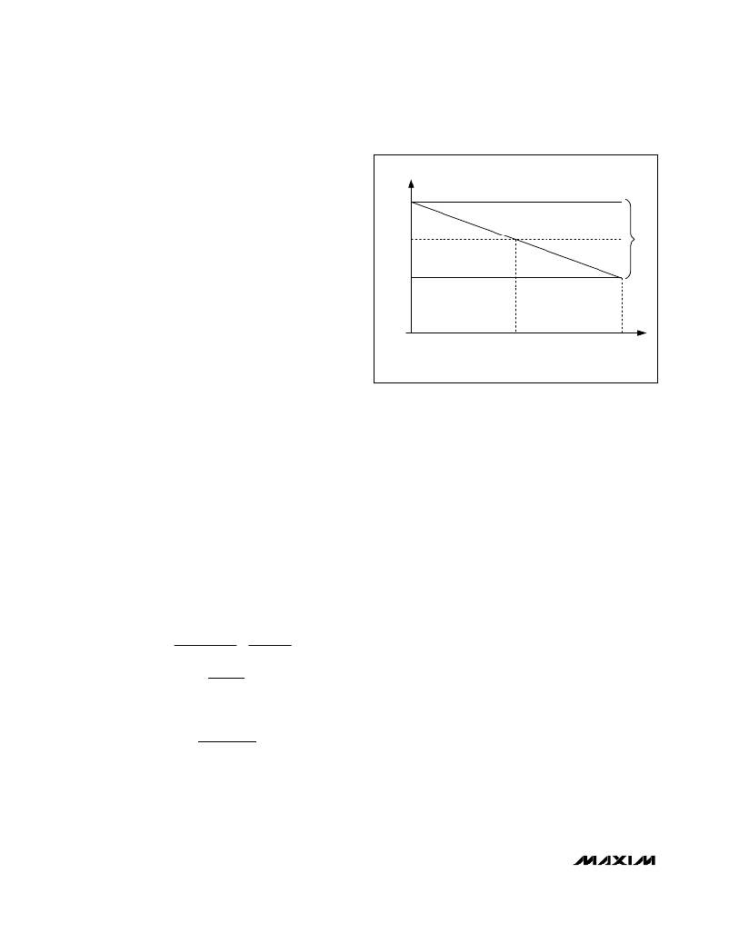
�NO� LOAD�
�1/2� LOAD�
�LOAD� (A)�
�FULL� LOAD�
�capacitors� to� meet� a� given� transient� response� require-�
�ment.� Setting� the� no-load� output� voltage� slightly� higher�
�than� the� output� voltage� during� nominally� loaded� condi-�
�tions� allows� a� larger� downward-voltage� excursion� when�
�the� output� current� suddenly� increases.� Regulating� at� a�
�lower� output� voltage� under� a� heavy� load� allows� a� larger�
�upward-voltage� excursion� when� the� output� current� sud-�
�denly� decreases.� Allowing� a� larger� voltage-step� excur-�
�sion� reduces� the� required� number� of� output� capacitors�
�or� allows� for� the� use� of� higher� ESR� capacitors.�
�Voltage� positioning� may� require� the� output� to� regulate�
�away� from� a� center� value.� Define� the� center� value� as�
�the� voltage� where� the� output� drops� (� ?� V� OUT� /2)� at� one�
�half� the� maximum� output� current� (Figure� 7).�
�Set� the� voltage-positioning� window� (� ?� V� OUT� )� using� the�
�resistive� feedback� of� the� voltage-error� amplifier� (VEA).�
�Use� the� following� equations� to� calculate� the� voltage-�
�positioning� window� (Figure� 5):�
�MAX5060:�
�Figure� 7.� Defining� the� Voltage-Positioning� Window�
�MOSFET� Gate� Drivers� (DH_,� DL_)�
�The� high-side� (DH)� and� low-side� (DL)� drivers� drive� the�
�gates� of� external� n-channel� MOSFETs� (Figures� 1� and� 2).�
�The� drivers’� 4A� peak� sink-� and� source-current� capability�
�provides� ample� drive� for� the� fast� rise� and� fall� times� of� the�
�switching� MOSFETs.� Faster� rise� and� fall� times� result� in�
�reduced� cross-conduction� losses.� For� modern� CPU� volt-�
�age-regulating� module� applications,� where� the� duty�
�cycle� is� less� than� 50%,� choose� high-side� MOSFETs� (Q1)�
�with� a� moderate� R� DS(ON)� and� a� very� low� gate� charge.�
�Choose� low-side� MOSFETs� (Q2)� with� very� low� R� DS(ON)�
�and� moderate� gate� charge.� Size� the� high-side� and� low-�
�side� MOSFETs� to� handle� the� peak� and� RMS� currents�
�during� overload� conditions.�
�The� driver� block� also� includes� a� logic� circuit� that� provides�
�� H� L�
�G� C� =�
�MAX5061:�
�?� V� OUT� =�
�I� OUT� � R� IN� R� +� R�
�G� C� � R� F� R� L�
�0� .� 0289�
�R� S�
�an� adaptive� nonoverlap� time� to� prevent� shoot-through�
�currents� during� transition.� The� typical� nonoverlap� time� is�
�35ns� between� the� high-side� and� low-side� MOSFETs.�
�BST�
�The� MAX5060� uses� V� DD� to� power� the� low-� and� high-side�
�MOSFET� drivers.� The� low-� and� high-side� drivers� in� the�
�MAX5061� are� powered� from� V� CC� .� The� high-side� driver�
�?� V� OUT� =� OUT� H�
�I� x� R�
�G� c� x� R� F�
�R� IN� and� R� F� are� the� input� and� feedback� resistors� of�
�VEA.� G� C� is� the� current-loop� transconductance� and� R� S�
�is� the� current-sense� resistor.�
�derives� its� power� through� a� bootstrap� capacitor� and� V� DD�
�supplies� power� internally� to� the� low-side� driver.� Connect� a�
�0.47μF� low-ESR� ceramic� capacitor� between� BST� and� LX.�
�Connect� a� Schottky� rectifier� from� BST� to� V� DD� on� the�
�MAX5060,� or� to� V� CC� on� the� MAX5061.� Reduce� the� PC�
�board� area� formed� by� the� boost� capacitor� and� rectifier.�
�20�
�______________________________________________________________________________________�
�相关PDF资料 |
PDF描述 |
|---|---|
| MAX5065EAI+ | IC REG CTRLR BUCK PWM CM 28-SSOP |
| MAX5066AUI+T | IC REG CTRLR BUCK PWM CM 28TSSOP |
| MAX5068DAUE+ | IC REG CTRLR FLYBK ISO 16-TSSOP |
| MAX5069CAUE+ | IC REG CTRLR ISO PWM CM 16-TSSOP |
| MAX5070AAUA+T | IC REG CTRLR FLYBK DIV ISO 8UMAX |
相关代理商/技术参数 |
参数描述 |
|---|---|
| MAX5060ATI+ | 功能描述:DC/DC 开关控制器 .6-5.5V Parallelable Average-Current-Mode RoHS:否 制造商:Texas Instruments 输入电压:6 V to 100 V 开关频率: 输出电压:1.215 V to 80 V 输出电流:3.5 A 输出端数量:1 最大工作温度:+ 125 C 安装风格: 封装 / 箱体:CPAK |
| MAX5060ATI+T | 功能描述:DC/DC 开关控制器 .6-5.5V Parallelable Average-Current-Mode RoHS:否 制造商:Texas Instruments 输入电压:6 V to 100 V 开关频率: 输出电压:1.215 V to 80 V 输出电流:3.5 A 输出端数量:1 最大工作温度:+ 125 C 安装风格: 封装 / 箱体:CPAK |
| MAX5060ATI-T | 功能描述:DC/DC 开关控制器 .6-5.5V Parallelable Average-Current-Mode RoHS:否 制造商:Texas Instruments 输入电压:6 V to 100 V 开关频率: 输出电压:1.215 V to 80 V 输出电流:3.5 A 输出端数量:1 最大工作温度:+ 125 C 安装风格: 封装 / 箱体:CPAK |
| MAX5060ETI | 功能描述:DC/DC 开关控制器 RoHS:否 制造商:Texas Instruments 输入电压:6 V to 100 V 开关频率: 输出电压:1.215 V to 80 V 输出电流:3.5 A 输出端数量:1 最大工作温度:+ 125 C 安装风格: 封装 / 箱体:CPAK |
| MAX5060ETI+ | 功能描述:DC/DC 开关控制器 .6-5.5V Parallelable Average-Current-Mode RoHS:否 制造商:Texas Instruments 输入电压:6 V to 100 V 开关频率: 输出电压:1.215 V to 80 V 输出电流:3.5 A 输出端数量:1 最大工作温度:+ 125 C 安装风格: 封装 / 箱体:CPAK |
发布紧急采购,3分钟左右您将得到回复。