- 您现在的位置:买卖IC网 > PDF目录17226 > MAX5060EVKIT (Maxim Integrated Products)EVAL KIT FOR MAX5060 PDF资料下载
参数资料
| 型号: | MAX5060EVKIT |
| 厂商: | Maxim Integrated Products |
| 文件页数: | 25/31页 |
| 文件大小: | 0K |
| 描述: | EVAL KIT FOR MAX5060 |
| 产品培训模块: | Lead (SnPb) Finish for COTS Obsolescence Mitigation Program |
| 标准包装: | 1 |
| 主要目的: | DC/DC,步降 |
| 输出及类型: | 1,非隔离 |
| 输出电压: | 3.3V |
| 电流 - 输出: | 20A |
| 输入电压: | 10 ~ 14V |
| 稳压器拓扑结构: | 降压 |
| 频率 - 开关: | 270kHz |
| 板类型: | 完全填充 |
| 已供物品: | 板 |
| 已用 IC / 零件: | MAX5060 |
第1页第2页第3页第4页第5页第6页第7页第8页第9页第10页第11页第12页第13页第14页第15页第16页第17页第18页第19页第20页第21页第22页第23页第24页当前第25页第26页第27页第28页第29页第30页第31页
�� �
�
�0.6V� to� 5.5V� Output,� Parallelable,�
�Average-Current-Mode� DC-DC� Controllers�
�(� I� DC� +� I� PK� +� I� )�
�I� RMS� ?� HI� =�
�DC� PK� �
�� I�
�(� ?� V� ESR� )�
�ESR� IN� =�
�?� I� OUT� +�
�?� ?� I� L� ?�
�?�
�2� ?�
�I� OUT� � D� (� 1� ?� D� )�
�C� IN� =�
�2� 2� D�
�3�
�where� D� =� V� OUT� /V� IN� ,� I� DC� =� (I� OUT� -� ?� I� L� /2)� and� I� PK� =�
�(I� OUT� +� ?� I� L� /2).�
�PD� MOS� ?� LO� =� (� Q� G� � V� DD� � f� SW� )� +�
�?�
�?� V� Q� � f� SW�
�where� I� OUT� is� the� output� current� of� the� converter.�
�?� 2� � C�
�(�
�� V� 2� � f�
�?�
�?� +� 1� .� 4� R� DS� (� ON� )� � I� RMS� ?� LO�
�?�
�?�
�?�
�(� I� DC� +� I� PK� +� I�
�)�
�2� 2� (� 1� ?� D� )�
�I� RMS� ?� LO� =� DC� � I� PK� �
�3�
�OSS� IN� SW� 2�
�3�
�)�
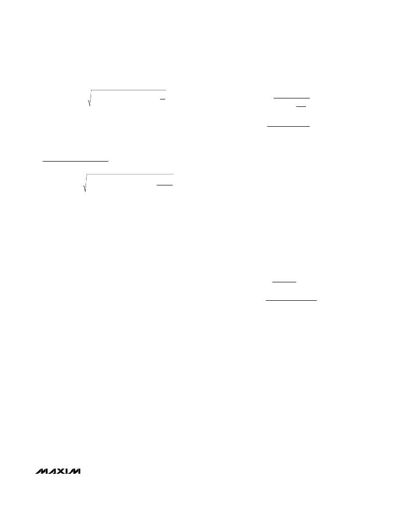
�For� example,� at� V� OUT� =� 1.8V,� the� ESR� and� input� capac-�
�itance� are� calculated� for� the� input� peak-to-peak� ripple�
�of� 100mV� or� less� yielding� an� ESR� and� capacitance�
�value� of� 1.25m� ?� and� 110μF.�
�Output� Capacitors�
�The� worst-case� peak-to-peak� and� capacitor� RMS� ripple�
�?� V� OESR�
�?� I� L�
�C� OUT� =�
�where� C� OSS� is� the� MOSFET� drain-to-source� capaci-�
�tance.�
�For� example,� from� the� typical� specifications� in� the�
�Applications� Information� section� with� V� OUT� =� 1.8V,� the�
�high-side� and� low-side� MOSFET� RMS� currents� are� 7.8A�
�and� 18.5A,� respectively� for� 20A.� Ensure� that� the� ther-�
�mal� impedance� of� the� MOSFET� package� keeps� the�
�junction� temperature� at� least� +25°C� below� the� absolute�
�maximum� rating.� Use� the� following� equation� to� calcu-�
�late� maximum� junction� temperature:�
�T� J� =� (PD� MOS� x� θ� JA� )� +� T� A�
�where� θ� JA� and� T� A� are� the� junction-to-ambient� thermal�
�impedance� and� ambient� temperature,� respectively.�
�Input� Capacitors�
�The� discontinuous� input-current� waveform� of� the� buck�
�converter� causes� large� ripple� currents� in� the� input� capac-�
�itor.� The� switching� frequency,� peak� inductor� current,� and�
�the� allowable� peak-to-peak� voltage� ripple� reflected� back�
�to� the� source� dictate� the� capacitance� requirement.�
�Increasing� switching� frequency� or� paralleling� multiple� out-�
�of-phase� converters� lowers� the� peak-to-average� current�
�ratio,� yielding� a� lower� input� capacitance� requirement� for�
�the� same� load� current.�
�The� input� ripple� is� comprised� of� ?� V� Q� (caused� by� the�
�capacitor� discharge)� and� ?� V� ESR� (caused� by� the� ESR� of�
�the� capacitor).� Use� low-ESR� ceramic� capacitors� with�
�high-ripple-current� capability� at� the� input.� Assume� the�
�contributions� from� the� ESR� and� capacitor� discharge� are�
�equal� to� 30%� and� 70%,� respectively.� Calculate� the� input�
�capacitance� and� ESR� required� for� a� specified� ripple�
�using� the� following� equation:�
�current,� the� allowable� peak-to-peak� output� ripple� volt-�
�age,� and� the� maximum� deviation� of� the� output� voltage�
�during� step� loads� determine� the� capacitance� and� the�
�ESR� requirements� for� the� output� capacitors.�
�In� buck� converter� design,� the� output-current� waveform�
�is� continuous� and� this� reduces� peak-to-peak� ripple� cur-�
�rent� in� the� output� capacitor� equal� to� the� inductor� ripple�
�current.� Calculate� the� capacitance,� the� ESR� of� the� out-�
�put� capacitor,� and� the� RMS� ripple� current� rating� of� the�
�output� capacitor� based� on� the� following� equations.�
�ESR� OUT� =�
�?� I� L�
�8� � ?� V� OQ� � f� SW�
�where� ?� V� OESR� and� ?� V� OQ� are� the� output-ripple� contri-�
�butions� due� to� ESR� and� the� discharge� of� output� capaci-�
�tor,� respectively.�
�In� the� dynamic� load� environment,� the� allowable� devia-�
�tion� of� output� voltage� during� the� fast� transient� load� dic-�
�tates� the� output� capacitance� and� ESR.� The� output�
�capacitors� supply� the� load� step� until� the� controller�
�responds� with� a� greater� duty� cycle.� The� response� time�
�(t� RESPONSE� )� depends� on� the� closed-loop� bandwidth� of�
�the� converter.� The� resistive� drop� across� the� capacitor�
�ESR� and� capacitor� discharge� causes� a� voltage� drop�
�during� a� step� load.� Use� a� combination� of� SP� polymer�
�and� ceramic� capacitors� for� better� transient� load� and�
�ripple/noise� performance.�
�______________________________________________________________________________________�
�25�
�相关PDF资料 |
PDF描述 |
|---|---|
| R1S8-1505/P | CONV DC/DC 1W 15VIN 05VOUT |
| GCA14DCBN | CONN EDGECARD 28POS R/A .125 SLD |
| R1S-2409/P | CONV DC/DC 1W 24VIN 09VOUT |
| GCA14DCBD | CONN EDGECARD 28POS R/A .125 SLD |
| R1S-153.3/P | CONV DC/DC 1W 15VIN 3.3VOUT |
相关代理商/技术参数 |
参数描述 |
|---|---|
| MAX5061 | 制造商:MAXIM 制造商全称:Maxim Integrated Products 功能描述:0.6V to 5.5V Output, Parallelable, Average-Current-Mode DC-DC Controllers |
| MAX5061AUE | 功能描述:DC/DC 开关控制器 .6-5.5V Parallelable Average-Current-Mode RoHS:否 制造商:Texas Instruments 输入电压:6 V to 100 V 开关频率: 输出电压:1.215 V to 80 V 输出电流:3.5 A 输出端数量:1 最大工作温度:+ 125 C 安装风格: 封装 / 箱体:CPAK |
| MAX5061AUE+ | 功能描述:DC/DC 开关控制器 .6-5.5V Parallelable Average-Current-Mode RoHS:否 制造商:Texas Instruments 输入电压:6 V to 100 V 开关频率: 输出电压:1.215 V to 80 V 输出电流:3.5 A 输出端数量:1 最大工作温度:+ 125 C 安装风格: 封装 / 箱体:CPAK |
| MAX5061AUE+T | 功能描述:DC/DC 开关控制器 .6-5.5V Parallelable Average-Current-Mode RoHS:否 制造商:Texas Instruments 输入电压:6 V to 100 V 开关频率: 输出电压:1.215 V to 80 V 输出电流:3.5 A 输出端数量:1 最大工作温度:+ 125 C 安装风格: 封装 / 箱体:CPAK |
| MAX5061AUE-T | 功能描述:DC/DC 开关控制器 .6-5.5V Parallelable Average-Current-Mode RoHS:否 制造商:Texas Instruments 输入电压:6 V to 100 V 开关频率: 输出电压:1.215 V to 80 V 输出电流:3.5 A 输出端数量:1 最大工作温度:+ 125 C 安装风格: 封装 / 箱体:CPAK |
发布紧急采购,3分钟左右您将得到回复。