- 您现在的位置:买卖IC网 > PDF目录15487 > MAX5069DAUE+ (Maxim Integrated Products)IC REG CTRLR ISO PWM CM 16-TSSOP PDF资料下载
参数资料
| 型号: | MAX5069DAUE+ |
| 厂商: | Maxim Integrated Products |
| 文件页数: | 12/19页 |
| 文件大小: | 0K |
| 描述: | IC REG CTRLR ISO PWM CM 16-TSSOP |
| 产品培训模块: | Lead (SnPb) Finish for COTS Obsolescence Mitigation Program |
| 标准包装: | 96 |
| PWM 型: | 电流模式 |
| 输出数: | 2 |
| 频率 - 最大: | 2.5MHz |
| 占空比: | 100% |
| 电源电压: | 10.8 V ~ 24 V |
| 降压: | 无 |
| 升压: | 无 |
| 回扫: | 无 |
| 反相: | 无 |
| 倍增器: | 无 |
| 除法器: | 无 |
| Cuk: | 无 |
| 隔离: | 是 |
| 工作温度: | -40°C ~ 125°C |
| 封装/外壳: | 16-TSSOP(0.173",4.40mm)裸露焊盘 |
| 包装: | 管件 |
�� �
�
�High-Frequency,� Current-Mode� PWM� Controller�
�with� Accurate� Oscillator� and� Dual� FET� Drivers�
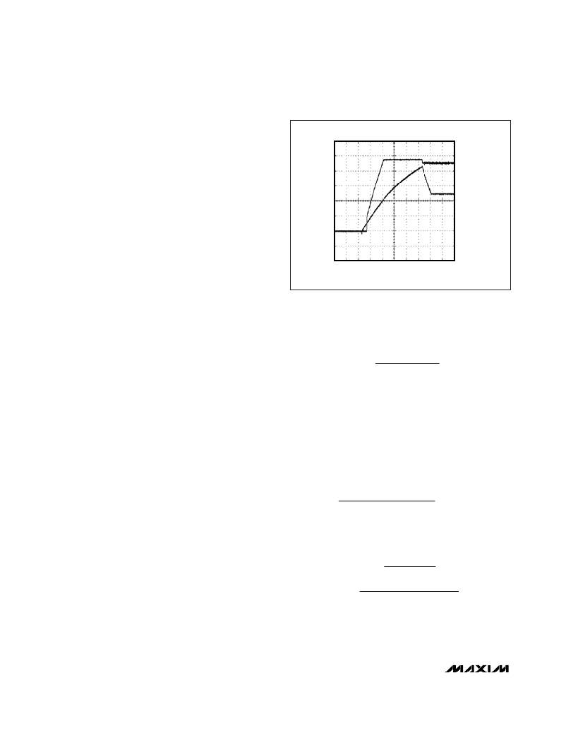
�MAX5069A/B� Startup� Operation�
�Normally,� V� IN� is� derived� from� the� tertiary� winding� of� the�
�transformer.� However,� at� startup� there� is� no� energy�
�delivered� through� the� transformer;� hence,� a� special�
�bootstrap� sequence� is� required.� Figure� 5� shows� the�
�voltages� on� V� IN� and� V� CC� during� startup.� Initially,� both�
�V� IN� and� V� CC� are� 0V.� After� the� input� voltage� is� applied,�
�C1� charges� through� the� startup� resistor,� R1,� to� an� inter-�
�mediate� voltage� (see� Figure� 1).� At� this� point,� the� inter-�
�nal� regulator� begins� charging� C3� (see� Figure� 5).� Only�
�47μA� of� the� current� supplied� by� R1� is� used� by� the�
�MAX5069A/B.� The� remaining� input� current� charges� C1�
�and� C3.� The� charging� of� C3� stops� when� the� V� CC� volt-�
�age� reaches� approximately� 9.5V.� The� voltage� across�
�C1� continues� rising� until� it� reaches� the� wake-up� level� of�
�23.6V.� Once� V� IN� exceeds� the� bootstrap� UVLO� thresh-�
�old,� NDRVA/NDRVB� begin� switching� the� MOSFETs� and�
�energy� is� transferred� to� the� secondary� and� tertiary� out-�
�puts.� If� the� voltage� on� the� tertiary� output� builds� to� high-�
�er� than� 9.74V� (the� bootstrap� UVLO� lower� threshold),�
�startup� ends� and� sustained� operation� commences.�
�If� V� IN� drops� below� 9.74V� before� startup� is� complete,� the�
�device� goes� back� to� low-current� UVLO.� If� this� occurs,�
�increase� the� value� of� C1� to� store� enough� energy� to�
�allow� for� the� voltage� at� the� tertiary� winding� to� build� up.�
�Startup� Time� Considerations� for�
�Power� Supplies� Using� the� MAX5069A/B�
�The� V� IN� bypass� capacitor,� C1,� supplies� current� imme-�
�diately� after� wakeup� (see� Figure� 1).� The� size� of� C1� and�
�the� connection� configuration� of� the� tertiary� winding�
�determine� the� number� of� cycles� available� for� startup.�
�Large� values� of� C1� increase� the� startup� time� and� also�
�supply� extra� gate� charge� for� more� cycles� during� initial�
�V� CC�
�2V/div�
�MAX5069�
�V� IN� PIN�
�5V/div�
�0V�
�100ms/div�
�Figure� 5.� V� IN� and� V� CC� During� Startup� When� Using� the�
�MAX5069� in� Bootstrapped� Mode� (See� Figure� 1)�
�I� g� =� Q� gtot� x� f� SW�
�(I� IN� +� I� g� ) x t� SS�
�C� 1� =�
�V� HYST�
�where� I� IN� is� the� MAX5069’s� internal� supply� current� after�
�startup� (3.3mA,� typ),� Q� gtot� is� the� total� gate� charge� for�
�Q1� and� Q2,� f� SW� is� the� MAX5069’s� programmed� output�
�switching� frequency,� V� HYST� is� the� bootstrap� UVLO� hys-�
�teresis� (12V),� and� t� ss� is� the� internal� soft-start� time� (2047�
�clock� cycles� x� 1� /� f� OSC� ).�
�Example:� I� g� =� (16nC)� (250kHz)� ?� 4mA�
�=� 2� .� 5� μ� F�
�startup.� If� the� value� of� C1� is� too� small,� V� IN� drops� below�
�9.74V� because� NDRVA/NDRVB� do� not� have� enough�
�time� to� switch� and� build� up� sufficient� voltage� across� the�
�tertiary� output� that� powers� the� device.� The� device� goes�
�back� into� UVLO� and� does� not� start.� Use� low-leakage�
�capacitors� for� C1� and� C3.�
�C� 1� =�
�f� OSC� =� 500kHz�
�t� SS� =� 2047� x� (1� /� f� OSC� )� =� 4.1ms�
�(3.3mA� +� 4mA ) (4.1ms)�
�12� V�
�Generally,� offline� power� supplies� keep� typical� startup�
�times� to� less� than� 500ms,� even� in� low-line� conditions�
�(85VAC� input� for� universal� offline� applications� or�
�Use� a� 4.7μF� ceramic� capacitor� for� C1.�
�Assuming� C1� >� C3,� calculate� the� value� of� R1� as� follows:�
�V� SUVR� � C� 1�
�I� C� 1� ?�
�36VDC� for� telecom� applications).� Size� the� startup� resis-�
�tor,� R1,� to� supply� both� the� maximum� startup� bias� of� the�
�device� (90μA)� and� the� charging� current� for� C1� and� C3.�
�The� bypass� capacitor,� C3,� must� charge� to� 9.5V,� and�
�C1� must� charge� to� 24V,� within� the� desired� time� period�
�of� 500ms.� Because� of� the� internal� soft-start� time� of� the�
�R� 1� ?�
�500� ms�
�V� IN� (� MIN� )� ?� 0� .� 5� x� V� SUVR�
�I� C� 1� +� I� START�
�MAX5069,� C1� must� store� enough� charge� to� deliver� cur-�
�rent� to� the� device� for� at� least� 2047� oscillator� clock�
�cycles.� To� calculate� the� approximate� amount� of� capaci-�
�tance� required,� use� the� following� formula:�
�where� V� SUVR� is� the� bootstrap� UVLO� wakeup� level�
�(23.6V� max),� V� IN(MIN)� is� the� minimum� input� supply� volt-�
�age� for� the� application� (36V� for� telecom),� and� I� START� is�
�the� V� IN� supply� current� at� startup� (90μA,� max).�
�12�
�______________________________________________________________________________________�
�相关PDF资料 |
PDF描述 |
|---|---|
| MAX1745AUB+ | IC REG CTRLR BUCK PWM 10-UMAX |
| SPD74-684M | INDUCTOR SHIELDED 680.0UH SMD |
| SPD74-683M | INDUCTOR SHIELDED 68.0UH SMD |
| UES1C471MHM | CAP ALUM 470UF 16V 20% RADIAL |
| SPD74-682M | INDUCTOR SHIELDED 6.80UH SMD |
相关代理商/技术参数 |
参数描述 |
|---|---|
| MAX5069DAUE+ | 功能描述:电流型 PWM 控制器 High-Frequency Current-Mode PWM RoHS:否 制造商:Texas Instruments 开关频率:27 KHz 上升时间: 下降时间: 工作电源电压:6 V to 15 V 工作电源电流:1.5 mA 输出端数量:1 最大工作温度:+ 105 C 安装风格:SMD/SMT 封装 / 箱体:TSSOP-14 |
| MAX5069DAUE+T | 功能描述:电流型 PWM 控制器 High-Frequency Current-Mode PWM RoHS:否 制造商:Texas Instruments 开关频率:27 KHz 上升时间: 下降时间: 工作电源电压:6 V to 15 V 工作电源电流:1.5 mA 输出端数量:1 最大工作温度:+ 105 C 安装风格:SMD/SMT 封装 / 箱体:TSSOP-14 |
| MAX5069DAUE-T | 功能描述:电流型 PWM 控制器 High-Frequency Current-Mode PWM RoHS:否 制造商:Texas Instruments 开关频率:27 KHz 上升时间: 下降时间: 工作电源电压:6 V to 15 V 工作电源电流:1.5 mA 输出端数量:1 最大工作温度:+ 105 C 安装风格:SMD/SMT 封装 / 箱体:TSSOP-14 |
| MAX5069EVKIT | 功能描述:电源管理IC开发工具 MAX5069 Eval Kit RoHS:否 制造商:Maxim Integrated 产品:Evaluation Kits 类型:Battery Management 工具用于评估:MAX17710GB 输入电压: 输出电压:1.8 V |
| MAX506ACPP | 功能描述:数模转换器- DAC RoHS:否 制造商:Texas Instruments 转换器数量:1 DAC 输出端数量:1 转换速率:2 MSPs 分辨率:16 bit 接口类型:QSPI, SPI, Serial (3-Wire, Microwire) 稳定时间:1 us 最大工作温度:+ 85 C 安装风格:SMD/SMT 封装 / 箱体:SOIC-14 封装:Tube |
发布紧急采购,3分钟左右您将得到回复。