- 您现在的位置:买卖IC网 > PDF目录20685 > MAX5092BATE+ (Maxim Integrated)IC REG DL BUCK/LINEAR 16TQFN PDF资料下载
参数资料
| 型号: | MAX5092BATE+ |
| 厂商: | Maxim Integrated |
| 文件页数: | 9/24页 |
| 文件大小: | 0K |
| 描述: | IC REG DL BUCK/LINEAR 16TQFN |
| 产品培训模块: | Lead (SnPb) Finish for COTS Obsolescence Mitigation Program |
| 标准包装: | 60 |
| 拓扑: | 降压(降压)(1),线性(LDO)(1) |
| 功能: | 车载 |
| 输出数: | 2 |
| 频率 - 开关: | 1MHz |
| 电压/电流 - 输出 1: | 7V/可调至11V,250mA |
| 电压/电流 - 输出 2: | 5V/1.5 V ~ 9 V,250mA |
| 带 LED 驱动器: | 无 |
| 带监控器: | 无 |
| 带序列发生器: | 无 |
| 电源电压: | 3.5 V ~ 72 V |
| 工作温度: | -40°C ~ 125°C |
| 安装类型: | 表面贴装 |
| 封装/外壳: | 16-WQFN 裸露焊盘 |
| 供应商设备封装: | 16-TQFN-EP(5x5) |
| 包装: | 管件 |
�� �
�
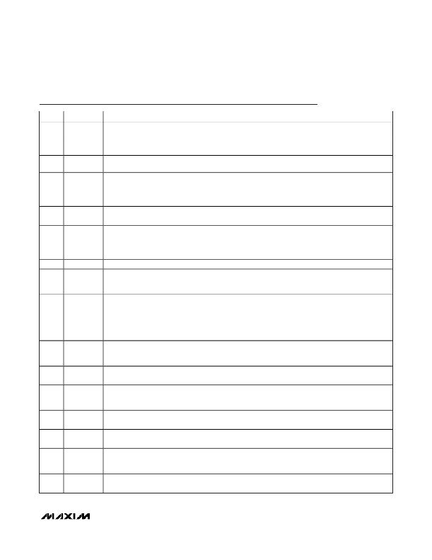
�4V� to� 72V� Input� LDOs� with� Boost� Preregulator�
�Pin� Description�
�PIN�
�1�
�2�
�3�
�4�
�5�
�6�
�NAME�
�IN�
�EN�
�SGND�
�HOLD�
�PGND_LDO�
�SET�
�FUNCTION�
�Input� Supply� Voltage.� Bypass� IN� to� the� power� ground� plane� with� a� 47μF� (low-ESR)� aluminum� electrolytic�
�capacitor� in� parallel� with� a� 1μF� ceramic� capacitor� placed� as� close� to� the� IC� as� possible.�
�Enable� Input.� Drive� EN� high� to� turn� on� the� IC.� Drive� EN� low� to� disable� the� IC.� Connect� EN� directly� to� IN� for�
�always-on� operation.�
�Signal� Ground.� Connect� SGND� to� the� signal� ground� plane� and� the� exposed� paddle.� Connect� the� power�
�ground� and� signal� ground� plane� together� at� the� negative� terminal� of� the� input� capacitor(s).�
�Output� Hold.� When� HOLD� is� forced� low,� the� regulator� stores� the� on-state� of� the� output,� allowing� the�
�regulator� to� remain� enabled� even� if� EN� is� pulled� low.� To� shut� down� the� regulator,� release� HOLD� after� EN� is�
�pulled� low.� If� HOLD� is� unused,� either� connect� HOLD� to� OUT� or� leave� unconnected.� HOLD� is� internally�
�connected� to� OUT� through� a� 4μA� pullup� current.�
�LDO� Power� Ground.� Connect� PGND_LDO� to� the� power� ground� plane.� Connect� the� PGND_LDO� ground� and�
�signal� ground� plane� together.�
�Feedback� Input� for� the� LDO.� Connect� SET� directly� to� SGND� to� set� the� output� voltage� of� the� LDO� to� the�
�preset� voltage� of� 3.3V� (MAX5092A/MAX5093A)� or� 5V� (MAX5092B/MAX5093B).� Connect� SET� to� the� center�
�tap� of� a� resistor-divider� connected� between� the� LDO� output� and� SGND� to� set� the� output� voltage.� V� SET�
�regulates� to� 1.24V� when� using� an� adjustable� output.�
�7�
�OUT_SENSE� LDO� Regulator� Output� Sense.� Connect� OUT_SENSE� to� OUT� at� the� output� capacitor� near� the� load.�
�LDO� Regulator� Output.� Bypass� OUT� to� the� power� ground� plane� with� a� 10μF� ceramic� capacitor.� V� OUT�
�8�
�9�
�10,� 11�
�12�
�13�
�14�
�15�
�16�
�—�
�OUT�
�BSOUT�
�LX�
�PGND_BST�
�BSFB�
�VL�
�CT�
�RESET�
�EP�
�regulates� to� a� preset� voltage� of� 3.3V� (MAX5092A/MAX5093A)� or� 5V� (MAX5092B/MAX5093B),� or� is�
�adjustable� from� 1.5V� to� 9V� (MAX5902_)� or� 1.5V� to� 10V� (MAX5093_).�
�Boost� Regulator� Output� Voltage.� Bypass� BSOUT� to� the� PGND_BST� ground� plane� with� a� 22μF� (low-ESR)�
�aluminum� electrolytic� capacitor� in� parallel� with� a� 1μF� ceramic� capacitor� placed� as� close� to� the� IC� as�
�possible.� Connect� BSFB� directly� to� SGND� to� regulate� the� BOOST� output� to� a� fixed� voltage� of� 7V� for� V� IN� ≤�
�7V.� V� BSOUT� follows� V� IN� for� V� BSOUT� -� V� OUT� >� 2.5V� (typ).� V� BSOUT� is� programmable� up� to� 11V� (MAX5092_)� or�
�12V� (MAX5093_)� by� connecting� BSFB� to� the� center� tap� of� an� external� resistor-divider� connected� between�
�the� BOOST� output� and� PGND_BST.�
�Inductor� Connection� to� the� Drain� of� the� Internal� Power� MOSFET.� Connect� LX� to� the� switched� side� of� the�
�inductor.� Connect� pins� 10� and� 11� together� as� close� to� the� device� as� possible.� For� the� MAX5093,� also�
�connect� LX� to� the� anode� of� the� external� Schottky� diode.�
�Boost� Regulator� Power� Ground.� Connect� PGND_BST� to� the� power� ground� plane.� Connect� the� PGND_BST�
�ground� plane� and� the� signal� ground� plane� together� at� the� negative� terminal� of� the� input� capacitor(s).�
�Feedback� Input� for� the� Boost� Regulator.� Connect� BSFB� directly� to� SGND� to� set� the� boost� regulator� output�
�voltage� to� 7V.� Connect� BSFB� to� the� center� tap� of� an� external� resistor-divider� connected� between� BSOUT�
�and� SGND� to� set� the� output� voltage.� V� BSFB� regulates� to� 1.24V� when� using� an� adjustable� output.�
�Internal� Regulator� Output� for� IC� Supply.� Bypass� VL� to� SGND� with� a� 1μF/6.3V� ceramic� capacitor� placed� as�
�close� to� the� IC� as� possible.� V� VL� regulates� to� 5.5V� with� V� BSOUT� ≥� 5.5V.�
�RESET� Timeout� Programming� Input.� Connect� a� capacitor� from� CT� to� SGND� to� set� the� RESET� timeout�
�period.� See� the� CT� Capacitor� Selection� section.�
�RESET� Output.� RESET� is� an� open-drain� output� that� goes� high� impedance� when� V� OUT� exceeds� 92%� of� the�
�output� voltage� threshold� after� a� programmed� time� delay.� RESET� pulls� low� immediately� once� V� OUT� drops�
�below� 90%� of� the� regulated� LDO� output� voltage.�
�Exposed� Paddle.� Connect� to� the� signal� ground� plane� (SGND).� Connect� to� a� large-signal� ground� plane� for�
�increased� thermal� performance.�
�_______________________________________________________________________________________�
�9�
�相关PDF资料 |
PDF描述 |
|---|---|
| S1BHE3/61T | DIODE GPP 1A 100V SMA DO-214AC |
| AD8213WYRMZ-RL | IC CURRENT MONITOR 0.25% 10MSOP |
| ABC40DRES-S734 | CONN EDGECARD 80POS .100 EYELET |
| RMM43DRMI-S288 | CONN EDGECARD 86POS .156 EXTEND |
| ECC09DJXB | CONN EDGECARD 18PS .100 PRESSFIT |
相关代理商/技术参数 |
参数描述 |
|---|---|
| MAX5092BATE+ | 功能描述:低压差稳压器 - LDO 4V to 72V LDO RoHS:否 制造商:Texas Instruments 最大输入电压:36 V 输出电压:1.4 V to 20.5 V 回动电压(最大值):307 mV 输出电流:1 A 负载调节:0.3 % 输出端数量: 输出类型:Fixed 最大工作温度:+ 125 C 安装风格:SMD/SMT 封装 / 箱体:VQFN-20 |
| MAX5092BATE+T | 功能描述:低压差稳压器 - LDO 4V to 72V LDO RoHS:否 制造商:Texas Instruments 最大输入电压:36 V 输出电压:1.4 V to 20.5 V 回动电压(最大值):307 mV 输出电流:1 A 负载调节:0.3 % 输出端数量: 输出类型:Fixed 最大工作温度:+ 125 C 安装风格:SMD/SMT 封装 / 箱体:VQFN-20 |
| MAX5092EVKIT+ | 功能描述:电源管理IC开发工具 MAX5092A-B/93A-B Eval Kit RoHS:否 制造商:Maxim Integrated 产品:Evaluation Kits 类型:Battery Management 工具用于评估:MAX17710GB 输入电压: 输出电压:1.8 V |
| MAX5093 | 制造商:MAXIM 制造商全称:Maxim Integrated Products 功能描述:4V to 72V Input LDOs with Boost Preregulator |
| MAX5093AATE+ | 功能描述:低压差稳压器 - LDO 4V to 72V LDO RoHS:否 制造商:Texas Instruments 最大输入电压:36 V 输出电压:1.4 V to 20.5 V 回动电压(最大值):307 mV 输出电流:1 A 负载调节:0.3 % 输出端数量: 输出类型:Fixed 最大工作温度:+ 125 C 安装风格:SMD/SMT 封装 / 箱体:VQFN-20 |
发布紧急采购,3分钟左右您将得到回复。