- 您现在的位置:买卖IC网 > PDF目录14390 > MAX5098AATJ+ (Maxim Integrated Products)IC REG BUCK BST ADJ 1A/2A 32TQFN PDF资料下载
参数资料
| 型号: | MAX5098AATJ+ |
| 厂商: | Maxim Integrated Products |
| 文件页数: | 11/28页 |
| 文件大小: | 0K |
| 描述: | IC REG BUCK BST ADJ 1A/2A 32TQFN |
| 产品培训模块: | Lead (SnPb) Finish for COTS Obsolescence Mitigation Program |
| 标准包装: | 60 |
| 类型: | 降压(降压),升压(升压) |
| 输出类型: | 可调式 |
| 输出数: | 2 |
| 输出电压: | 0.8 V ~ 0.85 V,4.5 V ~ 28 V |
| 输入电压: | 4.5 V ~ 19 V |
| PWM 型: | 电压模式 |
| 频率 - 开关: | 200kHz ~ 2.2MHz |
| 电流 - 输出: | 1A,2A |
| 同步整流器: | 无 |
| 工作温度: | -40°C ~ 125°C |
| 安装类型: | 表面贴装 |
| 封装/外壳: | 32-WFQFN 裸露焊盘 |
| 包装: | 管件 |
| 供应商设备封装: | 32-TQFN-EP(5x5) |
第1页第2页第3页第4页第5页第6页第7页第8页第9页第10页当前第11页第12页第13页第14页第15页第16页第17页第18页第19页第20页第21页第22页第23页第24页第25页第26页第27页第28页
�� �
�
�Dual,� 2.2MHz,� Automotive� Buck� or� Boost�
�Converter� with� 80V� Load-Dump� Protection�
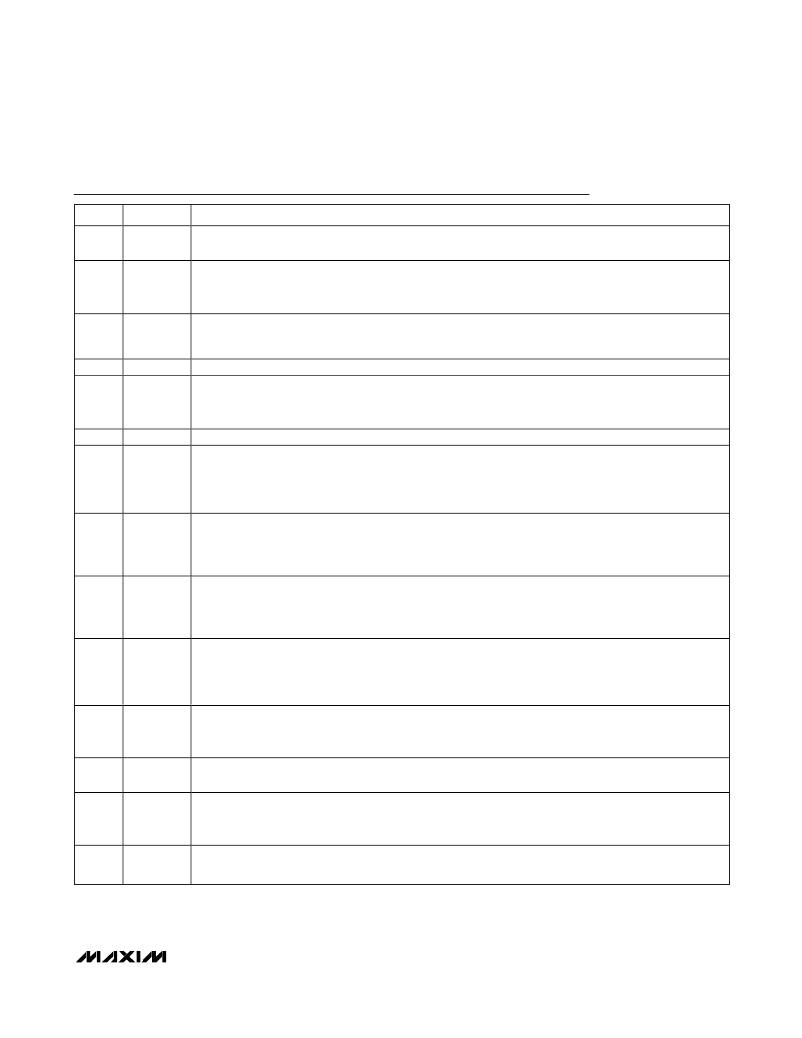
�Pin� Description�
�PIN�
�1,� 32�
�2,� 3�
�4�
�5�
�6�
�7�
�8�
�9�
�10�
�11�
�12�
�13�
�14�
�15�
�NAME�
�SOURCE2�
�DRAIN2�
�PGOOD2�
�EN2�
�FB2�
�COMP2�
�OSC�
�SYNC�
�GATE�
�ON/OFF�
�IN_HIGH�
�V+�
�V� L�
�SGND�
�FUNCTION�
�Converter� 2� Internal� MOSFET� Source� Connection.� For� buck� converter� operation,� connect� SOURCE2� to� the�
�switched� side� of� the� inductor.� For� boost� operation,� connect� SOURCE2� to� PGND_� (Figure� 6).�
�Converter� 2� Internal� MOSFET� Drain� Connection.� For� buck� converter� operation,� use� the� MOSFET� as� a� high-�
�side� switch� and� connect� DRAIN2� to� the� DC-DC� converters� supply� input� rail.� For� boost� converter� operation,�
�use� the� MOSFET� as� a� low-side� switch� and� connect� DRAIN2� to� the� inductor� and� diode� junction� (Figure� 6).�
�Converter� 2� Open-Drain� Power-Good� Output.� PGOOD2� goes� low� when� converter� 2’s� output� falls� below�
�92.5%� of� its� set� regulation� voltage.� Use� PGOOD2� and� EN1� to� sequence� the� converters.� Converter� 2� starts�
�first.�
�Converter� 2� Active-High� Enable� Input.� Connect� to� V� L� for� always-on� operation.�
�Converter� 2� Feedback� Input.� Connect� FB2� to� a� resistive� divider� between� converter� 2’s� output� and� SGND� to�
�adjust� the� output� voltage.� To� set� the� output� voltage� below� 0.8V,� connect� FB2� to� a� resistive� voltage-divider�
�from� BYPASS� to� regulator� 2’s� output� (Figure� 3).� See� the� Setting� the� Output� Voltage� section.�
�Converter� 2� Internal� Transconductance� Amplifier� Output.� See� the� Compensation� section.�
�Oscillator� Frequency� Set� Input.� Connect� a� resistor� from� OSC� to� SGND� (R� OSC� )� to� set� the� switching� frequency�
�(see� the� Setting� the� Switching� Frequency� section).� Set� R� OSC� for� an� oscillator� frequency� equal� to� the� SYNC�
�input� frequency� when� using� external� synchronization.� R� OSC� is� still� required� when� an� external� clock� is�
�connected� to� the� SYNC� input.� See� the� Synchronization� (SYNC)/Clock� Output� (CKO)� section.�
�External� Clock� Synchronization� Input.� Connect� SYNC� to� a� 400kHz� to� 4400kHz� clock� to� synchronize� the�
�switching� frequency� with� the� system� clock.� Each� converter� frequency� is� 1/2� of� the� frequency� applied� to�
�SYNC� (FSEL_1� =� V� L� ).� For� FSEL_1� =� SGND,� the� switching� frequency� of� converter� 1� becomes� 1/4� of� the�
�SYNC� frequency.� Connect� SYNC� to� SGND� when� not� used.�
�Gate� Drive� Output.� Connect� to� the� gate� of� the� external� n-channel� load-dump� protection� MOSFET.� GATE� =�
�IN_HIGH� +� 9V� (typ)� with� IN_HIGH� =� 12V.� GATE� pulls� to� IN_HIGH� by� an� internal� n-channel� MOSFET� when� V+�
�raises� 2V� above� IN_HIGH.� Leave� gate� unconnected� if� the� load-dump� protection� is� not� used� (MOSFET� not�
�installed).�
�n-Channel� Switch� Enable� Input.� Drive� ON/OFF� high� for� normal� operation.� Drive� ON/OFF� low� to� turn� off� the�
�external� n-channel� load-dump� protection� MOSFET� and� reduce� the� supply� current� to� 7μA� (typ).� When�
�ON/OFF� is� driven� low,� both� DC-DC� converters� are� disabled� and� the� PGOOD_� outputs� are� driven� low.�
�Connect� to� V+� if� the� external� load-dump� protection� is� not� used� (MOSFET� not� installed).�
�Startup� Input.� IN_HIGH� is� protected� by� internally� clamping� to� 21V� (max).� Connect� a� resistor� (4k� Ω� max)� from�
�IN_HIGH� to� the� drain� of� the� protection� switch.� Bypass� IN_HIGH� with� a� 4.7μF� electrolytic� or� 1μF� minimum�
�ceramic� capacitor.� Connect� to� V+� if� the� external� load-dump� protection� is� not� used� (MOSFET� not� installed).�
�Input� Supply� Voltage.� V+� can� range� from� 5.2V� to� 19V.� Connect� V+,� IN_HIGH,� and� V� L� together� for� 4.5V� to�
�5.5V� input� operation.� Bypass� V+� to� SGND� with� a� 1μF� minimum� ceramic� capacitor.�
�Internal� Regulator� Output.� The� V� L� regulator� is� used� to� supply� the� drive� current� at� input� VDRV.� When� driving�
�VDRV,� use� an� RC� lowpass� filter� to� decouple� switching� noise� from� VDRV� to� the� V� L� regulator� (see� the� Typical�
�Application� Circuit� ).� Bypass� V� L� to� SGND� with� a� 4.7μF� minimum� ceramic� capacitor.�
�Signal� Ground.� Connect� SGND� to� exposed� pad� and� to� the� board� signal� ground� plane.� Connect� the� board�
�signal� ground� and� power� ground� planes� together� at� a� single� point.�
�______________________________________________________________________________________�
�11�
�相关PDF资料 |
PDF描述 |
|---|---|
| RBM36DRUS | CONN EDGECARD 72POS DIP .156 SLD |
| VI-B5V-EX-F4 | CONVERTER MOD DC/DC 5.8V 75W |
| ECC35DRSD-S273 | CONN EDGECARD 70POS DIP .100 SLD |
| MAX5099ATJ+ | IC REG BUCK SYNC ADJ DL 32TQFN |
| EMM15DTMT-S189 | CONN EDGECARD 30POS R/A .156 SLD |
相关代理商/技术参数 |
参数描述 |
|---|---|
| MAX5098AATJ+ | 功能描述:直流/直流开关转换器 Dual 2.2MHz Buck or Boost Converter RoHS:否 制造商:STMicroelectronics 最大输入电压:4.5 V 开关频率:1.5 MHz 输出电压:4.6 V 输出电流:250 mA 输出端数量:2 最大工作温度:+ 85 C 安装风格:SMD/SMT |
| MAX5098AATJ+T | 功能描述:直流/直流开关转换器 Dual 2.2MHz Buck or Boost Converter RoHS:否 制造商:STMicroelectronics 最大输入电压:4.5 V 开关频率:1.5 MHz 输出电压:4.6 V 输出电流:250 mA 输出端数量:2 最大工作温度:+ 85 C 安装风格:SMD/SMT |
| MAX5099 | 制造商:MAXIM 制造商全称:Maxim Integrated Products 功能描述:Dual, 2.2MHz, Automotive Synchronous Buck Converter with 80V Load-Dump Protection |
| MAX5099ATJ | 制造商:MAXIM 制造商全称:Maxim Integrated Products 功能描述:Dual, 2.2MHz, Automotive Synchronous Buck Converter with 80V Load-Dump Protection |
| MAX5099ATJ+ | 功能描述:直流/直流开关转换器 Dual 2.2MHz Synch Buck Converter RoHS:否 制造商:STMicroelectronics 最大输入电压:4.5 V 开关频率:1.5 MHz 输出电压:4.6 V 输出电流:250 mA 输出端数量:2 最大工作温度:+ 85 C 安装风格:SMD/SMT |
发布紧急采购,3分钟左右您将得到回复。