- 您现在的位置:买卖IC网 > PDF目录8528 > MAX5259EEE+T (Maxim Integrated Products)IC DAC 8BIT OCTAL 3V 16-QSOP PDF资料下载
参数资料
| 型号: | MAX5259EEE+T |
| 厂商: | Maxim Integrated Products |
| 文件页数: | 7/20页 |
| 文件大小: | 0K |
| 描述: | IC DAC 8BIT OCTAL 3V 16-QSOP |
| 产品培训模块: | Lead (SnPb) Finish for COTS Obsolescence Mitigation Program |
| 标准包装: | 2,500 |
| 设置时间: | 10µs |
| 位数: | 8 |
| 数据接口: | 串行 |
| 转换器数目: | 8 |
| 电压电源: | 单电源 |
| 工作温度: | -40°C ~ 85°C |
| 安装类型: | 表面贴装 |
| 封装/外壳: | 16-SSOP(0.154",3.90mm 宽) |
| 供应商设备封装: | 16-QSOP |
| 包装: | 带卷 (TR) |
| 输出数目和类型: | 8 电压,单极 |
| 采样率(每秒): | * |
LDAC Operation (Hardware)
LDAC is typically used in 4-wire interfaces (Figure 4).
This command is level sensitive, and it allows asyn-
chronous hardware control of the DAC outputs. With
LDAC low, all eight DAC registers are transparent, and
any time an input register is updated, the DAC output
immediately follows.
Serial Data Output
DOUT is the internal shift-register’s output. DOUT can
be programmed to clock out data on the falling edge of
SCLK (mode 0) or the rising edge (mode 1). In mode 0,
output data lags input data by 16.5 clock cycles, main-
taining compatibility with MICROWIRE and SPI. In
mode 1, output data lags input data by 16 clock cycles.
On power-up, DOUT defaults to mode 0 timing. DOUT
never three-states; it always actively drives either high
or low and remains unchanged when CS is high.
Interfacing to the Microprocessor
The MAX5258/MAX5259 are MICROWIRE (Figure 5)
and SPI/QSPI (Figure 6) compatible. For SPI and QSPI,
clear the CPOL and CPHA configuration bits (CPOL =
CPHA = 0). The SPI/QSPI CPOL = CPHA = 1 configura-
tion can also be used if the DOUT output is ignored.
The MAX5258/MAX5259 can interface with Intel’s
80C5X/80C3X family in mode 0 if the SCLK clock polar-
ity is inverted. Universally, if a serial port is not avail-
able, three lines from one of the parallel ports can be
used for bit manipulation.
Digital feedthrough at the voltage outputs is greatly
minimized by operating the serial clock only to update
the registers. See the Clock Feedthrough photo in the
Typical Operating Characteristics section. The clock
idle state is low.
Daisy-Chaining Devices
Any number of MAX5258/MAX5259s can be daisy-
chained by connecting DOUT of one device to DIN of
the following device in the chain with all devices in
mode zero. The NOP instruction (Table 1) allows data
to be passed from DIN to DOUT without changing the
input or DAC registers of the passing device. A 3-wire
interface updates daisy-chained or individual
MAX5258/MAX5259s simultaneously by bringing CS
high (Figure 7).
Analog Section
DAC Operation
The MAX5258/MAX5259 use a matrix decoding archi-
tecture for the DACs, which saves power in the overall
system. The external reference voltage is divided down
by a resistor string placed in a matrix fashion. Row and
column decoders select the appropriate tab from the
resistor string to provide the needed analog voltages.
The resistor string presents a code-independent input
impedance to the reference and guarantees a monoto-
nic output. Figure 8 shows a simplified diagram of one
of the eight DACs.
Reference Input
The voltage at REF sets the full-scale output voltage for
all eight DACs. The 230k
typical input impedance at
REF is code independent. The output voltage for any
DAC can be represented by a digitally programmable
voltage source as follows:
VOUT = (NB VREF) / 256,
where NB is the numerical value of the DAC’s binary
input code.
Output Buffer Amplifiers
All MAX5258/MAX5259 voltage outputs are internally
buffered by precision unity-gain followers that slew at
about 0.55V/s. The outputs can swing from GND to
VDD. With a 0 to VREF (or VREF to 0) output transition,
the amplifier outputs will typically settle to 1/2LSB in
10s when loaded with 10k
in parallel with 100pF.
The buffer amplifiers are stable with any combination of
resistive (
≥10k) or capacitive (≤100pF) loads.
Applications Information
DAC Linearity and Voltage Offset
The output buffer can have a negative input offset volt-
age that would normally drive the output negative, but
since there is no negative supply, the output remains at
GND (Figure 9). When linearity is determined using the
endpoint method, it is measured between code 10 (0A
hex) and full-scale code (FF hex) after offset and gain
error are calibrated out. With a single-supply, negative
offset causes the output not to change with an input
code transition near zero (Figure 9). Thus, the lowest
code that produces a positive output is the lower end-
point.
MAX5258/MAX5259
+3V/+5V, Low-Power, 8-Bit Octal DAC
with Rail-to-Rail Output Buffers
______________________________________________________________________________________
15
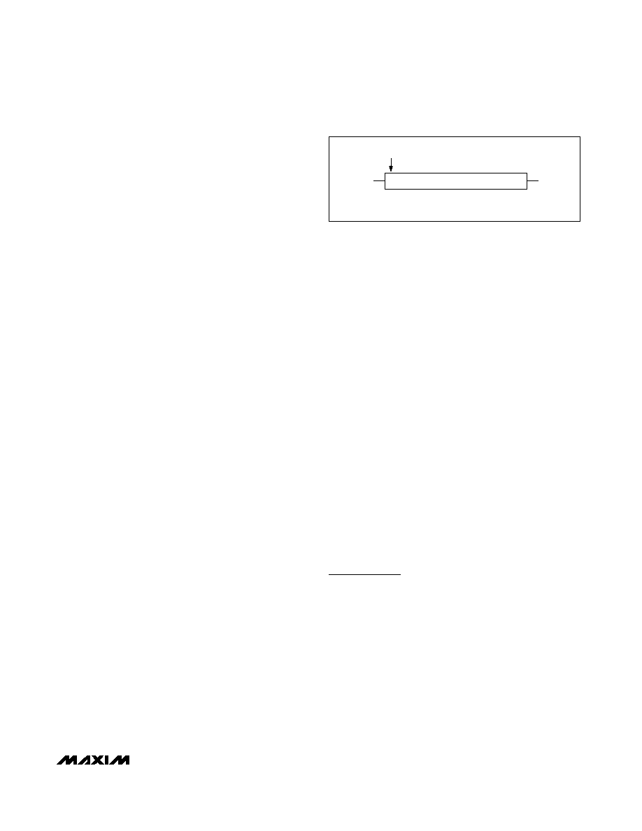
THIS IS THE FIRST BIT SHIFTED IN
DOUT
X X A2 A1 A0 C2 C1 C0 D7 D6 . . . D1 D0
DIN
MSB
LSB
8-BIT DAC DATA
CONTROL AND
ADDRESS BITS
Figure 3. Serial Input Format
相关PDF资料 |
PDF描述 |
|---|---|
| VE-B3F-MX-S | CONVERTER MOD DC/DC 72V 75W |
| MAX504CSD+T | IC DAC 10BIT VOLT OUT 14-SOIC |
| MAX5815BAUD+T | IC DAC 12BIT SRL 4CH 14TSSOP |
| VE-BNP-MU-F1 | CONVERTER MOD DC/DC 13.8V 200W |
| MAX522ESA+T | IC DAC 8BIT DUAL SERIAL 8-SOIC |
相关代理商/技术参数 |
参数描述 |
|---|---|
| MAX525AC | 制造商:Maxim Integrated Products 功能描述: |
| MAX525ACAP | 功能描述:数模转换器- DAC RoHS:否 制造商:Texas Instruments 转换器数量:1 DAC 输出端数量:1 转换速率:2 MSPs 分辨率:16 bit 接口类型:QSPI, SPI, Serial (3-Wire, Microwire) 稳定时间:1 us 最大工作温度:+ 85 C 安装风格:SMD/SMT 封装 / 箱体:SOIC-14 封装:Tube |
| MAX525ACAP+ | 功能描述:数模转换器- DAC 12-Bit 4Ch Precision DAC RoHS:否 制造商:Texas Instruments 转换器数量:1 DAC 输出端数量:1 转换速率:2 MSPs 分辨率:16 bit 接口类型:QSPI, SPI, Serial (3-Wire, Microwire) 稳定时间:1 us 最大工作温度:+ 85 C 安装风格:SMD/SMT 封装 / 箱体:SOIC-14 封装:Tube |
| MAX525ACAP+T | 功能描述:数模转换器- DAC 12-Bit 4Ch Precision DAC RoHS:否 制造商:Texas Instruments 转换器数量:1 DAC 输出端数量:1 转换速率:2 MSPs 分辨率:16 bit 接口类型:QSPI, SPI, Serial (3-Wire, Microwire) 稳定时间:1 us 最大工作温度:+ 85 C 安装风格:SMD/SMT 封装 / 箱体:SOIC-14 封装:Tube |
| MAX525ACAP-T | 功能描述:数模转换器- DAC RoHS:否 制造商:Texas Instruments 转换器数量:1 DAC 输出端数量:1 转换速率:2 MSPs 分辨率:16 bit 接口类型:QSPI, SPI, Serial (3-Wire, Microwire) 稳定时间:1 us 最大工作温度:+ 85 C 安装风格:SMD/SMT 封装 / 箱体:SOIC-14 封装:Tube |
发布紧急采购,3分钟左右您将得到回复。