- 您现在的位置:买卖IC网 > PDF目录10845 > MAX5316GTG+T (Maxim Integrated Products)IC DAC 16BIT SPI 24TQFN PDF资料下载
参数资料
| 型号: | MAX5316GTG+T |
| 厂商: | Maxim Integrated Products |
| 文件页数: | 13/33页 |
| 文件大小: | 0K |
| 描述: | IC DAC 16BIT SPI 24TQFN |
| 产品培训模块: | Obsolescence Mitigation Program |
| 标准包装: | 2,500 |
| 设置时间: | 3µs |
| 位数: | 16 |
| 数据接口: | DSP,MICROWIRE?,QSPI?,串行,SPI? |
| 转换器数目: | 1 |
| 电压电源: | 模拟和数字,双 ± |
| 功率耗散(最大): | 2.29W |
| 工作温度: | -40°C ~ 105°C |
| 安装类型: | 表面贴装 |
| 封装/外壳: | 24-VFQFN 裸露焊盘 |
| 供应商设备封装: | 24-TQFN-EP(4x5) |
| 包装: | 带卷 (TR) |
| 输出数目和类型: | 1 电压,单极;1 电压,双极 |
第1页第2页第3页第4页第5页第6页第7页第8页第9页第10页第11页第12页当前第13页第14页第15页第16页第17页第18页第19页第20页第21页第22页第23页第24页第25页第26页第27页第28页第29页第30页第31页第32页第33页
20
MAX5316
16-Bit, ±1 LSB Accuracy Voltage Output
DAC with SPI Interface
Detailed Description
The MAX5316 is a high-accuracy, 16-bit, serial SPI input,
buffered voltage output digital-to-analog converter (DAC) in
a 4mm x 5mm, 24-lead TQFN package. The device features
Q
1 LSB INL (max) accuracy and a Q1 LSB DNL (max) accu-
racy over the -40NC to +105NC temperature range.
The DAC voltage output is buffered with a fast set-
tling time of 3Fs and a low offset and gain drift of
Q
0.6ppm/NC of FSR (typ). The force-sense output (OUT)
maintains accuracy while driving loads with long lead
lengths. A separate AVSS supply allows the output amplifier
to go to 0V (GND) while maintaining full linearity performance.
At power-up, the device resets its outputs to zero or mid-
scale, providing additional safety for applications which
drive valves or other transducers that need to be off on
power-up. This is selected by the state of the M/Z input
on power-up.
The wide supply voltage range of 2.7V to 5.5V and
integrated low-drift, low-noise reference buffer ampli-
fier makes for ease of use. Since the reference buffer
input has a high input resistance, an external buffer is
not required. The device accepts an external reference
between 2.4V and VAVDD - 0.1V for maximum flexibility.
The MAX5316 features a 50MHz, 3-wire SPI, QSPI,
MICROWIRE, and DSP-compatible serial interface. The
separate digital interface supply voltage input (VDDIO) is
compatible with a wide range of digital logic levels from 1.7V
to 5.5V, eliminating the need for separate voltage translators.
DAC Reference Buffer
The external reference input has a high input (REF) imped-
ance of 10MI || 10pF and accepts an input voltage from
+2.4V to VAVDD - 0.1V. Connect an external reference
supply between REF and AGND. Bypass the reference
buffer output REFO to AGND with a 100pF capacitor.
Connect the anode of an external Schottky diode to REF
and the cathode to AVDD1 to prevent internal ESD diode
conduction in the event that the reference voltage comes
up before AVDD at power up. Follow the recommenda-
tions described in the Power-Supply Sequencing section.
Visit www.maxim-ic.com/products/references for a list
of available external voltage-reference devices.
Output Amplifier (OUT)
The MAX5316 includes an internal buffer for the DAC
output. The internal buffer provides improved load
regulation for the DAC output. The output buffer slews at
5V/Fs and can drive up to 2kI in parallel with 200pF.
The buffer has a rail-to-rail output capable of swinging to
within 100mV of AVDD_ and AVSS.
The positive analog supply voltage (AVDD_) determines
the maximum output voltage of the device as AVDD_
powers the output buffer.
The output is diode clamped to ground, preventing nega-
tive voltage excursions beyond approximately -0.6V.
Negative Supply Voltage (AVSS)
The negative supply voltage (AVSS) determines the minmum
output voltage. If AVSS is connected to ground, the output
voltage can be set to as low as 100mV without degrading
linearity. For operation down to 0V, connect AVSS to a nega-
tive supply voltage between -0.1V and -1.25V. The MAX1735
is recommended for generating -1.25V from a -5V supply.
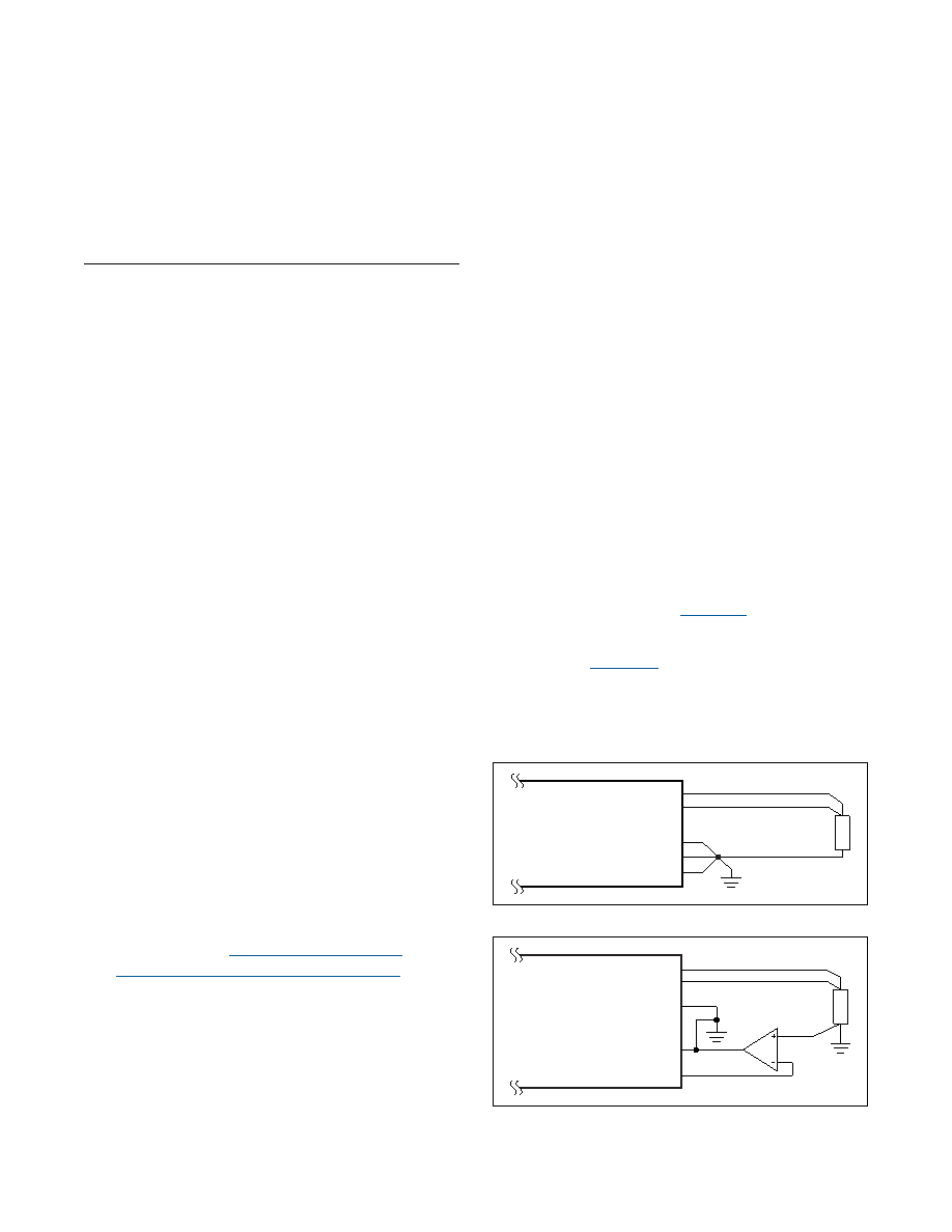
Force/Sense
The MAX5316 uses force/sense techniques to ensure
that the load is regulated to the desired output volt-
age despite line drops due to long lead lengths. Since
AGND_F and AGND_S have code dependent ground
currents, a ground impedance less than 13mω ensures
that the INL will not degrade by more than 0.1 LSB. Form
a star ground connection (Figure 2a) near the device
with AGND_F, AGND_S, and AGND tied together. Always
refer remote DAC loads to this system ground for best
performance. Figure 2b shows how to configure the
device and an external op amp for proper force/sense
operation. The amplifier provides as much drive as
needed to force the sensed voltage (measured between
RFB and AGND_S) to equal the desired voltage.
Figure 2a. Star Ground Connection
Figure 2b. Force/Sense Connection
OUT
RFB
AGND_F
AGND_S
AGND
MAX5316
OUT
RFB
AGND
AGND_F
AGND_S
MAX5316
相关PDF资料 |
PDF描述 |
|---|---|
| RM12BRB-7PH | CONN RECEPT 7POS PIN SILVER |
| VE-214-IX | CONVERTER MOD DC/DC 48V 75W |
| VE-21K-IX | CONVERTER MOD DC/DC 40V 75W |
| 1811902-3 | CONN PLUG SZ19 B KEY 4POS CRIMP |
| 1811901-1 | CONN RCPT SZ19 PNL MT N KEY 4POS |
相关代理商/技术参数 |
参数描述 |
|---|---|
| MAX5317GTG+ | 功能描述:数模转换器- DAC 16Bit DAC w/Digital Gain/Offset Control RoHS:否 制造商:Texas Instruments 转换器数量:1 DAC 输出端数量:1 转换速率:2 MSPs 分辨率:16 bit 接口类型:QSPI, SPI, Serial (3-Wire, Microwire) 稳定时间:1 us 最大工作温度:+ 85 C 安装风格:SMD/SMT 封装 / 箱体:SOIC-14 封装:Tube |
| MAX5317GTG+T | 功能描述:数模转换器- DAC 16Bit DAC w/Digital Gain/Offset Control RoHS:否 制造商:Texas Instruments 转换器数量:1 DAC 输出端数量:1 转换速率:2 MSPs 分辨率:16 bit 接口类型:QSPI, SPI, Serial (3-Wire, Microwire) 稳定时间:1 us 最大工作温度:+ 85 C 安装风格:SMD/SMT 封装 / 箱体:SOIC-14 封装:Tube |
| MAX5318GTG+ | 功能描述:数模转换器- DAC 18-bit V Out SPI DAC w/Digi Gain & Offset RoHS:否 制造商:Texas Instruments 转换器数量:1 DAC 输出端数量:1 转换速率:2 MSPs 分辨率:16 bit 接口类型:QSPI, SPI, Serial (3-Wire, Microwire) 稳定时间:1 us 最大工作温度:+ 85 C 安装风格:SMD/SMT 封装 / 箱体:SOIC-14 封装:Tube |
| MAX5318GTG+T | 功能描述:数模转换器- DAC 18-bit V Out SPI DAC w/Digi Gain & Offset RoHS:否 制造商:Texas Instruments 转换器数量:1 DAC 输出端数量:1 转换速率:2 MSPs 分辨率:16 bit 接口类型:QSPI, SPI, Serial (3-Wire, Microwire) 稳定时间:1 us 最大工作温度:+ 85 C 安装风格:SMD/SMT 封装 / 箱体:SOIC-14 封装:Tube |
| MAX5318GUG+ | 功能描述:数模转换器- DAC 18-BIT VOLTAGE OUTPUT SPI DAC RoHS:否 制造商:Texas Instruments 转换器数量:1 DAC 输出端数量:1 转换速率:2 MSPs 分辨率:16 bit 接口类型:QSPI, SPI, Serial (3-Wire, Microwire) 稳定时间:1 us 最大工作温度:+ 85 C 安装风格:SMD/SMT 封装 / 箱体:SOIC-14 封装:Tube |
发布紧急采购,3分钟左右您将得到回复。