- 您现在的位置:买卖IC网 > PDF目录9179 > MAX5489EUD+T (Maxim Integrated Products)IC POT DGTL DUAL 256-TAP 14TSSOP PDF资料下载
参数资料
| 型号: | MAX5489EUD+T |
| 厂商: | Maxim Integrated Products |
| 文件页数: | 12/13页 |
| 文件大小: | 0K |
| 描述: | IC POT DGTL DUAL 256-TAP 14TSSOP |
| 产品培训模块: | Lead (SnPb) Finish for COTS Obsolescence Mitigation Program |
| 标准包装: | 2,500 |
| 接片: | 256 |
| 电阻(欧姆): | 100k |
| 电路数: | 2 |
| 温度系数: | 标准值 35 ppm/°C |
| 存储器类型: | 非易失 |
| 接口: | 3 线串行(芯片选择) |
| 电源电压: | 2.7 V ~ 5.25 V |
| 工作温度: | -40°C ~ 85°C |
| 安装类型: | 表面贴装 |
| 封装/外壳: | 14-TSSOP(0.173",4.40mm 宽) |
| 供应商设备封装: | 14-TSSOP |
| 包装: | 带卷 (TR) |
MAX5487/MAX5488/MAX5489
Dual, 256-Tap, Nonvolatile, SPI-Interface,
Linear-Taper Digital Potentiometers
8
_______________________________________________________________________________________
Detailed Description
The MAX5487/MAX5488/MAX5489 contain two resistor
arrays, with 255 resistive elements each. The MAX5487
has an end-to-end resistance of 10k
, while the
MAX5488 and MAX5489 have resistances of 50k
and
100k
, respectively. The MAX5487/MAX5488/MAX5489
allow access to the high, low, and wiper terminals on
both potentiometers for a standard voltage-divider con-
figuration. Connect the wiper to the high terminal, and
connect the low terminal to ground, to make the device
a variable resistor (see Figure 1).
A simple 3-wire serial interface programs either wiper
directly to any of the 256 tap points. The nonvolatile
memory stores the wiper position prior to power-down
and recalls the wiper to the same point upon power-up
or by using an interface command (see Table 1). The
nonvolatile memory is guaranteed for 200,000 wiper
store cycles and 50 years for wiper data retention.
SPI Digital Interface
The MAX5487/MAX5488/MAX5489 use a 3-wire SPI-
compatible serial data interface (Figures 2 and 3). This
write-only interface contains three inputs: chip-select
(
CS), data clock (SCLK), and data in (DIN). Drive CS low
to enable the serial interface and clock data synchro-
nously into the shift register on each SCLK rising edge.
The WRITE commands (C1, C0 = 00 or 01) require 16
clock cycles to clock in the command, address, and data
(Figure 3a). The COPY commands (C1, C0 = 10, 11) can
use either eight clock cycles to transfer only command
and address bits (Figure 3b) or 16 clock cycles, with the
device disregarding 8 data bits (Figure 3a).
After loading data into the shift register, drive
CS high
to latch the data into the appropriate potentiometer
control register and disable the serial interface. Keep
CS low during the entire serial data stream to avoid cor-
ruption of the data.
Digital-Interface Format
The data format consists of three elements: command
bits, address bits, and data bits (see Table 1 and
Figure 3). The command bits (C1 and C0) indicate the
action to be taken such as changing or storing the
wiper position. The address bits (A1 and A0) specify
which potentiometer the command affects and the 8
data bits (D7 to D0) specify the wiper position.
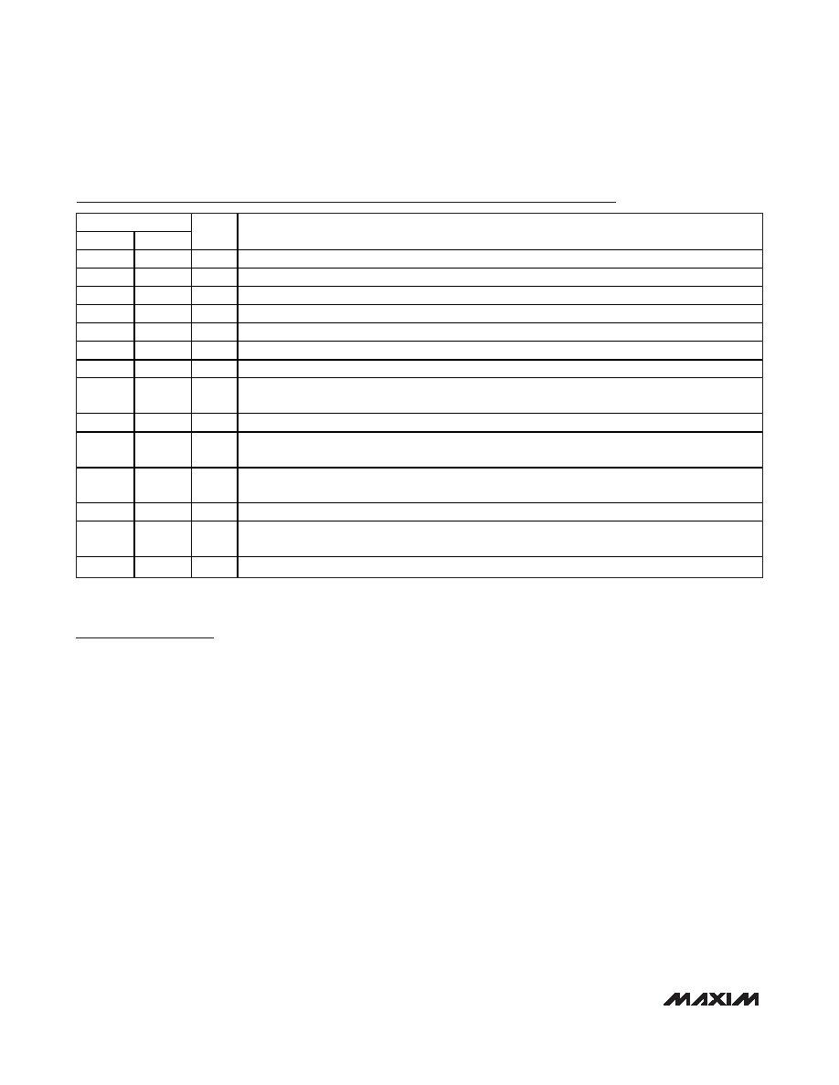
PIN
TQFN
TSSOP
NAME
FUNCTION
114
VDD
Power Supply. Bypass VDD to GND with a 0.1F capacitor as close to the device as possible.
2
13
SCLK
Serial-Interface Clock Input
3
12
DIN
Serial-Interface Data Input
411
CS
Active-Low Chip-Select Digital Input
5, 6, 9
7, 9, 10
N.C.
No Connection. Not internally connected.
7
8
GND
Ground
8, 16
—
I.C.
Internally connected to EP. Leave unconnected.
10
6
LB
Low Terminal of Resistor B. The voltage at L can be greater than or less than the voltage at H.
Current can flow into or out of L.
11
5
WB
Wiper Terminal of Resistor B
12
4
HB
High Terminal of Resistor B. The voltage at H can be greater than or less than the voltage at L.
Current can flow into or out of H.
13
3
LA
Low Terminal of Resistor A. The voltage at L can be greater than or less than the voltage at H.
Current can flow into or out of L.
14
2
WA
Wiper Terminal of Resistor A
15
1
HA
High Terminal of Resistor A. The voltage at H can be greater than or less than the voltage at L.
Current can flow into or out of H.
—
EP
Exposed Pad (TQFN only). Internally connected to pins 8 and 16. Leave unconnected.
Pin Description
相关PDF资料 |
PDF描述 |
|---|---|
| VE-2WP-MY-F2 | CONVERTER MOD DC/DC 13.8V 50W |
| V28A28H200BG3 | CONVERTER MOD DC/DC 28V 200W |
| VE-2WN-MY-F3 | CONVERTER MOD DC/DC 18.5V 50W |
| MAX5488EUD+T | IC POT DGTL DUAL 256-TAP 14TSSOP |
| VE-B11-MW-B1 | CONVERTER MOD DC/DC 12V 100W |
相关代理商/技术参数 |
参数描述 |
|---|---|
| MAX548AC/D | 功能描述:数模转换器- DAC RoHS:否 制造商:Texas Instruments 转换器数量:1 DAC 输出端数量:1 转换速率:2 MSPs 分辨率:16 bit 接口类型:QSPI, SPI, Serial (3-Wire, Microwire) 稳定时间:1 us 最大工作温度:+ 85 C 安装风格:SMD/SMT 封装 / 箱体:SOIC-14 封装:Tube |
| MAX548ACPA | 功能描述:数模转换器- DAC RoHS:否 制造商:Texas Instruments 转换器数量:1 DAC 输出端数量:1 转换速率:2 MSPs 分辨率:16 bit 接口类型:QSPI, SPI, Serial (3-Wire, Microwire) 稳定时间:1 us 最大工作温度:+ 85 C 安装风格:SMD/SMT 封装 / 箱体:SOIC-14 封装:Tube |
| MAX548ACPA+ | 功能描述:数模转换器- DAC 8-Bit 2Ch Precision DAC RoHS:否 制造商:Texas Instruments 转换器数量:1 DAC 输出端数量:1 转换速率:2 MSPs 分辨率:16 bit 接口类型:QSPI, SPI, Serial (3-Wire, Microwire) 稳定时间:1 us 最大工作温度:+ 85 C 安装风格:SMD/SMT 封装 / 箱体:SOIC-14 封装:Tube |
| MAX548ACUA | 功能描述:数模转换器- DAC RoHS:否 制造商:Texas Instruments 转换器数量:1 DAC 输出端数量:1 转换速率:2 MSPs 分辨率:16 bit 接口类型:QSPI, SPI, Serial (3-Wire, Microwire) 稳定时间:1 us 最大工作温度:+ 85 C 安装风格:SMD/SMT 封装 / 箱体:SOIC-14 封装:Tube |
| MAX548ACUA+ | 功能描述:数模转换器- DAC 8-Bit 2Ch Precision DAC RoHS:否 制造商:Texas Instruments 转换器数量:1 DAC 输出端数量:1 转换速率:2 MSPs 分辨率:16 bit 接口类型:QSPI, SPI, Serial (3-Wire, Microwire) 稳定时间:1 us 最大工作温度:+ 85 C 安装风格:SMD/SMT 封装 / 箱体:SOIC-14 封装:Tube |
发布紧急采购,3分钟左右您将得到回复。