- 您现在的位置:买卖IC网 > PDF目录9179 > MAX5489EUD+T (Maxim Integrated Products)IC POT DGTL DUAL 256-TAP 14TSSOP PDF资料下载
参数资料
| 型号: | MAX5489EUD+T |
| 厂商: | Maxim Integrated Products |
| 文件页数: | 8/13页 |
| 文件大小: | 0K |
| 描述: | IC POT DGTL DUAL 256-TAP 14TSSOP |
| 产品培训模块: | Lead (SnPb) Finish for COTS Obsolescence Mitigation Program |
| 标准包装: | 2,500 |
| 接片: | 256 |
| 电阻(欧姆): | 100k |
| 电路数: | 2 |
| 温度系数: | 标准值 35 ppm/°C |
| 存储器类型: | 非易失 |
| 接口: | 3 线串行(芯片选择) |
| 电源电压: | 2.7 V ~ 5.25 V |
| 工作温度: | -40°C ~ 85°C |
| 安装类型: | 表面贴装 |
| 封装/外壳: | 14-TSSOP(0.173",4.40mm 宽) |
| 供应商设备封装: | 14-TSSOP |
| 包装: | 带卷 (TR) |
MAX5487/MAX5488/MAX5489
Dual, 256-Tap, Nonvolatile, SPI-Interface,
Linear-Taper Digital Potentiometers
4
_______________________________________________________________________________________
Note 1: All devices are production tested at TA = +85°C and are guaranteed by design and characterization for -40°C < TA < +85°C.
Note 2: DNL and INL are measured with the potentiometer configured as a voltage-divider with H_ = VDD and L_ = 0. The wiper terminal
is unloaded and measured with an ideal voltmeter.
Note 3: DNL and INL are measured with the potentiometer configured as a variable resistor. H_ is unconnected and L_ = 0. For VDD =
+5V, the wiper terminal is driven with a source current of 400A for the 10k
configuration, 80A for the 50k configuration,
and 40A for the 100k
configuration. For VDD = +3V, the wiper terminal is driven with a source current of 200A for the 10k
configuration, 40A for the 50k
configuration, and 20A for the 100k configuration.
Note 4: The wiper resistance is the worst value measured by injecting the currents given in Note 3 into W_ with L_ = GND. RW =
(VW - VH) / IW.
Note 5: The device draws higher supply current when the digital inputs are driven with voltages between (VDD - 0.5V) and (GND +
0.5V). See Supply Current vs. Digital Input Voltage in the
Typical Operating Characteristics section.
Note 6: Wiper at midscale with a 10pF load.
Note 7: Wiper-settling time is the worst-case 0-to-50% rise time, measured between tap 0 and tap 127. H_ = VDD, L_ = GND, and
the wiper terminal is unloaded and measured with a 10pF oscilloscope probe (see Tap-to-Tap Switching Transient in the
Typical Operating Characteristics section).
Note 8: Digital timing is guaranteed by design and characterization, and is not production tested.
DC ELECTRICAL CHARACTERISTICS (continued)
(VDD = +2.7V to +5.25V, VH = VDD, VL = GND, TA = -40
°C to +85°C, unless otherwise noted. Typical values are at VDD = +5.0V,
TA = +25
°C, unless otherwise noted.) (Note 1)
PARAMETER
SYMBOL
CONDITIONS
MIN
TYP
MAX
UNITS
POWER SUPPLIES
Power-Supply Voltage
VDD
2.70
5.25
V
Supply Current
IDD
During write cycle only, digital inputs =
VDD or GND
400
A
Standby Current
Digital inputs = VDD or GND, TA = +25°C
0.5
1
A
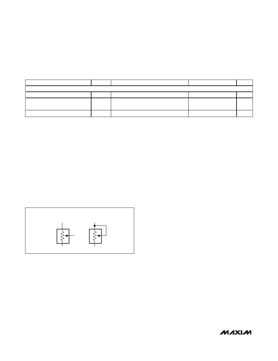
H
L
W
VOLTAGE-DIVIDER
CONFIGURATION
VARIABLE-RESISTOR
CONFIGURATION
H
L
Figure 1. Voltage-Divider/Variable-Resistor Configurations
相关PDF资料 |
PDF描述 |
|---|---|
| VE-2WP-MY-F2 | CONVERTER MOD DC/DC 13.8V 50W |
| V28A28H200BG3 | CONVERTER MOD DC/DC 28V 200W |
| VE-2WN-MY-F3 | CONVERTER MOD DC/DC 18.5V 50W |
| MAX5488EUD+T | IC POT DGTL DUAL 256-TAP 14TSSOP |
| VE-B11-MW-B1 | CONVERTER MOD DC/DC 12V 100W |
相关代理商/技术参数 |
参数描述 |
|---|---|
| MAX548AC/D | 功能描述:数模转换器- DAC RoHS:否 制造商:Texas Instruments 转换器数量:1 DAC 输出端数量:1 转换速率:2 MSPs 分辨率:16 bit 接口类型:QSPI, SPI, Serial (3-Wire, Microwire) 稳定时间:1 us 最大工作温度:+ 85 C 安装风格:SMD/SMT 封装 / 箱体:SOIC-14 封装:Tube |
| MAX548ACPA | 功能描述:数模转换器- DAC RoHS:否 制造商:Texas Instruments 转换器数量:1 DAC 输出端数量:1 转换速率:2 MSPs 分辨率:16 bit 接口类型:QSPI, SPI, Serial (3-Wire, Microwire) 稳定时间:1 us 最大工作温度:+ 85 C 安装风格:SMD/SMT 封装 / 箱体:SOIC-14 封装:Tube |
| MAX548ACPA+ | 功能描述:数模转换器- DAC 8-Bit 2Ch Precision DAC RoHS:否 制造商:Texas Instruments 转换器数量:1 DAC 输出端数量:1 转换速率:2 MSPs 分辨率:16 bit 接口类型:QSPI, SPI, Serial (3-Wire, Microwire) 稳定时间:1 us 最大工作温度:+ 85 C 安装风格:SMD/SMT 封装 / 箱体:SOIC-14 封装:Tube |
| MAX548ACUA | 功能描述:数模转换器- DAC RoHS:否 制造商:Texas Instruments 转换器数量:1 DAC 输出端数量:1 转换速率:2 MSPs 分辨率:16 bit 接口类型:QSPI, SPI, Serial (3-Wire, Microwire) 稳定时间:1 us 最大工作温度:+ 85 C 安装风格:SMD/SMT 封装 / 箱体:SOIC-14 封装:Tube |
| MAX548ACUA+ | 功能描述:数模转换器- DAC 8-Bit 2Ch Precision DAC RoHS:否 制造商:Texas Instruments 转换器数量:1 DAC 输出端数量:1 转换速率:2 MSPs 分辨率:16 bit 接口类型:QSPI, SPI, Serial (3-Wire, Microwire) 稳定时间:1 us 最大工作温度:+ 85 C 安装风格:SMD/SMT 封装 / 箱体:SOIC-14 封装:Tube |
发布紧急采购,3分钟左右您将得到回复。