- 您现在的位置:买卖IC网 > PDF目录10848 > MAX5856AECM+TD (Maxim Integrated Products)IC DAC 8BIT DUAL 300MSPS 48-TQFP PDF资料下载
参数资料
| 型号: | MAX5856AECM+TD |
| 厂商: | Maxim Integrated Products |
| 文件页数: | 11/23页 |
| 文件大小: | 0K |
| 描述: | IC DAC 8BIT DUAL 300MSPS 48-TQFP |
| 产品培训模块: | Lead (SnPb) Finish for COTS Obsolescence Mitigation Program |
| 标准包装: | 2,000 |
| 设置时间: | 11ns |
| 位数: | 8 |
| 数据接口: | 并联 |
| 转换器数目: | 2 |
| 电压电源: | 单电源 |
| 功率耗散(最大): | 792mW |
| 工作温度: | -40°C ~ 85°C |
| 安装类型: | 表面贴装 |
| 封装/外壳: | 48-TQFP 裸露焊盘 |
| 供应商设备封装: | 48-TQFP 裸露焊盘(7x7) |
| 包装: | 带卷 (TR) |
| 输出数目和类型: | 2 电流,单极 |
| 采样率(每秒): | 300M |
MAX5856A
Dual 8-Bit, 300Msps DAC with 4x/2x/1x
Interpolation Filters and PLL
______________________________________________________________________________________
19
CLKXP
1
CLK
DA0–DA7/
CONTROL WORD
tCXD
tDCSR
tDCHR
DAN
DBN
CONTROL WORD
DAN+1
DBN+1
1. CLKXP AND CLKXN MUST BE PRESENT ONLY WHEN PLL IS DISABLED, WITH PLLEN CONNECTED TO GND. THE DIAGRAM SHOWS 4x INTERPOLATION.
2. CLK IS AN OUTPUT WHEN PLL IS DISABLED, WITH PLLEN CONNECTED TO GND; OTHERWISE, IT IS AN INPUT.
CLKXN
1
tCWH
DB0–DB7
CW
tCXD
tCWS
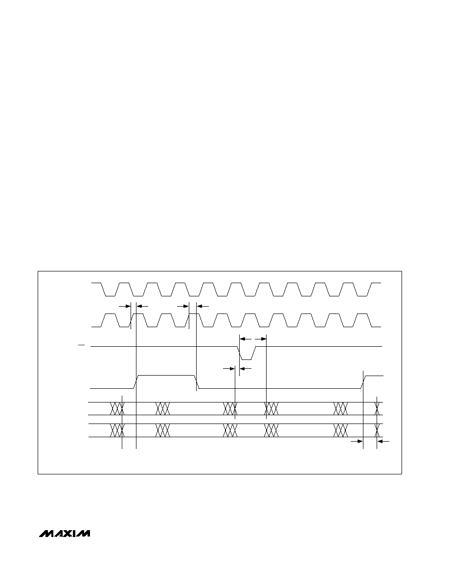
Figure 6. Timing Diagram for Noninterleave Data Mode (IDE = Low)
Figure 6 illustrates the DAC write cycle in 4x interpola-
tion mode. With the interpolation feature enabled, the
device can operate with the PLL enabled or disabled.
To obtain best phase noise performance, disable the
PLL and keep the capacitive load at the CLK output low
(10pF or less at fDAC = 165MHz).
With the PLL disabled (PLLEN = 0), the clock signal is
applied to CLKXP/CLKXN and internally divided by 4 to
generate the DAC’s CLK signal. The CLK signal is a
divide-by-4 output, used to synchronize data into the
MAX5856A data ports. The CLKXP/CLKXN signal dri-
ves the interpolation filters and DAC cores at the
desired conversion rate.
If the PLL is enabled (PLLEN = 1), then CLK becomes
an input and the clock signal may be applied to CLK. In
Figure 6, the CLK signal is multiplied by a factor of four
by the PLL and distributed to the interpolation filters
and DAC cores. In this mode, CLKXP must be pulled
low and CLKXN pulled high.
The MAX5856A can operate with a single-ended clock
input used as both data clock and conversion clock. To
operate the device in this mode, disable the interpolation
filters and enable the PLL (PLLEN = 1). Apply a single-
ended clock input at CLK. The CLK signal acts as the
data synchronization clock and DAC core conversion
clock. Though the PLL is enabled, the lock pin (LOCK) is
not valid and the PLL is internally disconnected from the
interpolating filters and DAC cores. In this mode, CLKXP
must be pulled low and CLKXN pulled high.
Figure 6 shows the timing for the CW. An 8-bit control
word routed through channel A’s data port programs
the gain matching, interpolator configuration, and oper-
ational mode of the MAX5856A. The control word is
latched on the falling edge of CW. The CW signal is
asynchronous with conversion clocks CLK and
CLKXN/CLKXP; therefore, the conversion clock (CLK or
CLKXN/CLKXP) can run uninterrupted when a control
word is written to the device.
相关PDF资料 |
PDF描述 |
|---|---|
| 1437720-9 | CONN RCPT SKT 8POS SLD CUP PNL |
| 7-1437719-8 | CONN RCPT SKT 8POS SLD PNL MNT |
| MAX5155BCEE+T | IC DAC 12BIT DUAL LP SER 16-QSOP |
| MAX5154BCEE+T | IC DAC 12BIT DUAL LP SER 16-QSOP |
| PIC17C766T-33I/L | IC MCU OTP 16KX16 A/D 84PLCC |
相关代理商/技术参数 |
参数描述 |
|---|---|
| MAX5858AECM | 制造商:Rochester Electronics LLC 功能描述: 制造商:Maxim Integrated Products 功能描述: |
| MAX5858AECM+D | 功能描述:数模转换器- DAC 10-Bit 2Ch 300Msps DAC RoHS:否 制造商:Texas Instruments 转换器数量:1 DAC 输出端数量:1 转换速率:2 MSPs 分辨率:16 bit 接口类型:QSPI, SPI, Serial (3-Wire, Microwire) 稳定时间:1 us 最大工作温度:+ 85 C 安装风格:SMD/SMT 封装 / 箱体:SOIC-14 封装:Tube |
| MAX5858AECM+TD | 功能描述:数模转换器- DAC 10-Bit 2Ch 300Msps DAC RoHS:否 制造商:Texas Instruments 转换器数量:1 DAC 输出端数量:1 转换速率:2 MSPs 分辨率:16 bit 接口类型:QSPI, SPI, Serial (3-Wire, Microwire) 稳定时间:1 us 最大工作温度:+ 85 C 安装风格:SMD/SMT 封装 / 箱体:SOIC-14 封装:Tube |
| MAX5858AECM-D | 功能描述:数模转换器- DAC RoHS:否 制造商:Texas Instruments 转换器数量:1 DAC 输出端数量:1 转换速率:2 MSPs 分辨率:16 bit 接口类型:QSPI, SPI, Serial (3-Wire, Microwire) 稳定时间:1 us 最大工作温度:+ 85 C 安装风格:SMD/SMT 封装 / 箱体:SOIC-14 封装:Tube |
| MAX5858AECM-TD | 功能描述:数模转换器- DAC RoHS:否 制造商:Texas Instruments 转换器数量:1 DAC 输出端数量:1 转换速率:2 MSPs 分辨率:16 bit 接口类型:QSPI, SPI, Serial (3-Wire, Microwire) 稳定时间:1 us 最大工作温度:+ 85 C 安装风格:SMD/SMT 封装 / 箱体:SOIC-14 封装:Tube |
发布紧急采购,3分钟左右您将得到回复。