- 您现在的位置:买卖IC网 > PDF目录10844 > MAX5858AECM+TD (Maxim Integrated Products)IC DAC 10BIT DUAL 300MSPS 48TQFP PDF资料下载
参数资料
| 型号: | MAX5858AECM+TD |
| 厂商: | Maxim Integrated Products |
| 文件页数: | 10/25页 |
| 文件大小: | 0K |
| 描述: | IC DAC 10BIT DUAL 300MSPS 48TQFP |
| 产品培训模块: | Lead (SnPb) Finish for COTS Obsolescence Mitigation Program |
| 标准包装: | 2,000 |
| 设置时间: | 11ns |
| 位数: | 10 |
| 数据接口: | 并联 |
| 转换器数目: | 2 |
| 电压电源: | 单电源 |
| 功率耗散(最大): | 816mW |
| 工作温度: | -40°C ~ 85°C |
| 安装类型: | 表面贴装 |
| 封装/外壳: | 48-TQFP 裸露焊盘 |
| 供应商设备封装: | 48-TQFP 裸露焊盘(7x7) |
| 包装: | 带卷 (TR) |
| 输出数目和类型: | 2 电流,单极 |
| 采样率(每秒): | 300M |
MAX5858A
Dual, 10-Bit, 300Msps, DAC with 4x/2x/1x
Interpolation Filters and PLL
18
______________________________________________________________________________________
IFS
CCOMP*
REFR
IREF
REFO
MAX4040
1.24V
BANDGAP
REFERENCE
CURRENT-
SOURCE ARRAY
*COMPENSATION CAPACITOR (CCOMP
≈ 100nF).
OPTIONAL EXTERNAL BUFFER
FOR HEAVIER LOADS
REN
MAX5858A
IREF =
VREF
RSET
AGND
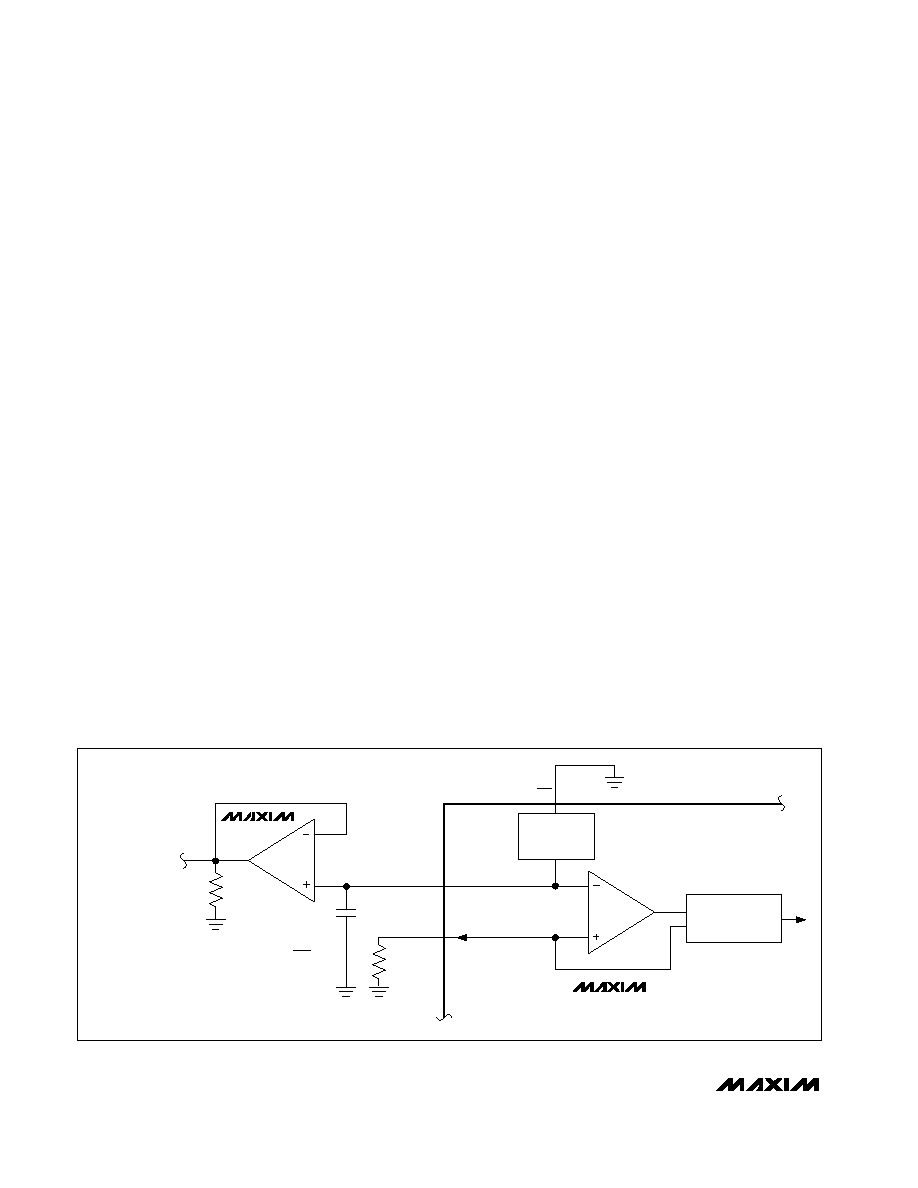
Figure 4. Setting IFS with the Internal 1.24V Reference and the Control Amplifier
PLL Clock Multiplier and
Clocking Modes
The MAX5858A features an on-chip PLL clock multiplier
that generates all internal, synchronized high-speed
clock signals required by the input data latches, inter-
polation filters, and DAC cores. The on-chip PLL
includes a phase-detector, VCO, prescalar, and
charge-pump circuits. The PLL can be enabled or dis-
abled through PLLEN. To enable PLL set PLLEN = 1.
With the PLL enabled (PLLEN = 1) and 4x/2x interpola-
tion enabled, an external low-frequency clock reference
source is applied to CLK pin. The clock reference
source serves as the input data clock. The on-chip PLL
multiplies the clock reference by a factor of two (2x) or
a factor of four (4x). The input data rate range and CLK
frequency are set by the selected interpolation mode.
In 2x interpolation mode, the data rate range is 75MHz
to 150MHz. In 4x interpolation mode the data rate
range is 37.5MHz to 75MHz.
Note: When the PLL is enabled, CLK becomes an
input, requiring CLKXP to be pulled low and CLKXN to
be pulled high. To obtain best phase noise perfor-
mance, disable the PLL function.
With the PLL disabled (PLLEN = 0) and 4x/2x interpola-
tion enabled, an external conversion clock is applied at
CLKXN/CLKXP. The conversion clock at CLKXN/CLKXP
has a frequency range of 0MHz to 300MHz (see Table
5). This clock is buffered and distributed by the
MAX5858A to drive the interpolation filters and DAC
cores. In this mode, CLK becomes a divide-by-N (DIV-
N) output at either a divide-by-two or divide-by-four
rate. The DIV-N factor is set by the selected interpola-
tion mode. The CLK output, at DIV-N rate, must be
used to synchronize data into the MAX5858A data
ports. In this mode, keep the capacitive load at the CLK
output low (10pF or less at fDAC = 165MHz).
With the interpolation disabled (1x mode) and the PLL
disabled (PLLEN = 0), the input clock at CLKXN/CLKXP
can be used to directly update the DAC cores. In this
mode, the maximum data rate is 165MHz.
Internal Reference and Control Amplifier
The MAX5858A provides an integrated 50ppm/°C,
1.24V, low-noise bandgap reference that can be dis-
abled and overridden with an external reference volt-
age. REFO serves either as an external reference input
or an integrated reference output. If REN is connected
to AGND, the internal reference is selected and REFO
provides a 1.24V (50A) output. Buffer REFO with an
external amplifier, when driving a heavy load.
The MAX5858A also employs a control amplifier
designed to simultaneously regulate the full-scale out-
put current (IFS) for both outputs of the devices.
Calculate the output current as:
IFS = 32 IREF
where IREF is the reference output current (IREF =
VREFO/RSET) and IFS is the full-scale output current. RSET
is the reference resistor that determines the amplifier out-
put current of the MAX5858A (Figure 4). This current is
mirrored into the current-source array where IFS is equally
distributed between matched current segments and
summed to valid output current readings for the DACs.
相关PDF资料 |
PDF描述 |
|---|---|
| MAX5207AEUB+T | IC DAC 16BIT SRL 10UMAX |
| MAX5206AEUB+T | IC DAC 16BIT SRL 10UMAX |
| HR34B-12WRB-4P | CONN RCPT 4POS MALE WALL MNT |
| HR34B-12WRA-10P | CONN RCPT 10POS MALE WALL MNT |
| RM12BRB-3S | CONN RECEPT 3POS SOCKET SILVER |
相关代理商/技术参数 |
参数描述 |
|---|---|
| MAX5858AEVKIT | 制造商:Maxim Integrated Products 功能描述:DUAL-10-BIT, 300MSPS, CURRENT-OUTPUT DAC WITH - Bulk |
| MAX5858ECM | 制造商:Rochester Electronics LLC 功能描述: 制造商:Maxim Integrated Products 功能描述: |
| MAX5858ECM+D | 功能描述:数模转换器- DAC 10-Bit 2Ch 300Msps DAC RoHS:否 制造商:Texas Instruments 转换器数量:1 DAC 输出端数量:1 转换速率:2 MSPs 分辨率:16 bit 接口类型:QSPI, SPI, Serial (3-Wire, Microwire) 稳定时间:1 us 最大工作温度:+ 85 C 安装风格:SMD/SMT 封装 / 箱体:SOIC-14 封装:Tube |
| MAX5858ECM+TD | 功能描述:数模转换器- DAC 10-Bit 2Ch 300Msps DAC RoHS:否 制造商:Texas Instruments 转换器数量:1 DAC 输出端数量:1 转换速率:2 MSPs 分辨率:16 bit 接口类型:QSPI, SPI, Serial (3-Wire, Microwire) 稳定时间:1 us 最大工作温度:+ 85 C 安装风格:SMD/SMT 封装 / 箱体:SOIC-14 封装:Tube |
| MAX5858ECM-D | 功能描述:数模转换器- DAC RoHS:否 制造商:Texas Instruments 转换器数量:1 DAC 输出端数量:1 转换速率:2 MSPs 分辨率:16 bit 接口类型:QSPI, SPI, Serial (3-Wire, Microwire) 稳定时间:1 us 最大工作温度:+ 85 C 安装风格:SMD/SMT 封装 / 箱体:SOIC-14 封装:Tube |
发布紧急采购,3分钟左右您将得到回复。