- 您现在的位置:买卖IC网 > PDF目录10844 > MAX5858AECM+TD (Maxim Integrated Products)IC DAC 10BIT DUAL 300MSPS 48TQFP PDF资料下载
参数资料
| 型号: | MAX5858AECM+TD |
| 厂商: | Maxim Integrated Products |
| 文件页数: | 12/25页 |
| 文件大小: | 0K |
| 描述: | IC DAC 10BIT DUAL 300MSPS 48TQFP |
| 产品培训模块: | Lead (SnPb) Finish for COTS Obsolescence Mitigation Program |
| 标准包装: | 2,000 |
| 设置时间: | 11ns |
| 位数: | 10 |
| 数据接口: | 并联 |
| 转换器数目: | 2 |
| 电压电源: | 单电源 |
| 功率耗散(最大): | 816mW |
| 工作温度: | -40°C ~ 85°C |
| 安装类型: | 表面贴装 |
| 封装/外壳: | 48-TQFP 裸露焊盘 |
| 供应商设备封装: | 48-TQFP 裸露焊盘(7x7) |
| 包装: | 带卷 (TR) |
| 输出数目和类型: | 2 电流,单极 |
| 采样率(每秒): | 300M |
MAX5858A
Dual, 10-Bit, 300Msps, DAC with 4x/2x/1x
Interpolation Filters and PLL
2
_______________________________________________________________________________________
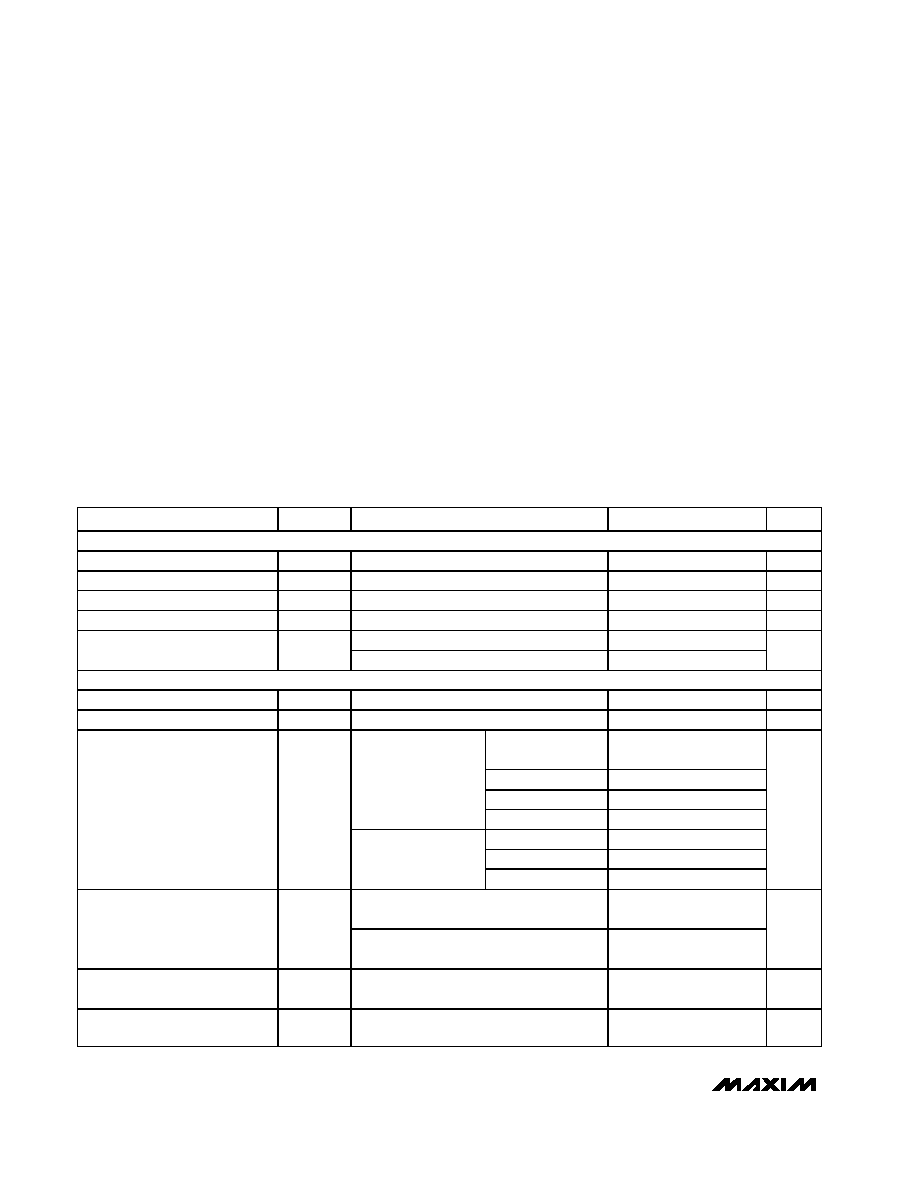
ABSOLUTE MAXIMUM RATINGS
ELECTRICAL CHARACTERISTICS
(AVDD = DVDD = PVDD = 3V, AGND = DGND = PGND = 0, fDAC = 165Msps, no interpolation, PLL disabled, external reference,
VREFO = 1.2V, IFS = 20mA, output amplitude = 0dB FS, differential output, TA = TMIN to TMAX, unless otherwise noted. TA > +25°C
guaranteed by production test. TA < +25°C guaranteed by design and characterization. Typical values are at TA = +25°C.)
Stresses beyond those listed under “Absolute Maximum Ratings” may cause permanent damage to the device. These are stress ratings only, and functional
operation of the device at these or any other conditions beyond those indicated in the operational sections of the specifications is not implied. Exposure to
absolute maximum rating conditions for extended periods may affect device reliability.
AVDD, DVDD, PVDD to AGND, DGND, PGND ..........-0.3V to +4V
DA9–DA0, DB9–DB0, CW, REN, PLLF, PLLEN to AGND,
DGND, PGND........................................................-0.3V to +4V
IDE to AGND, DGND, PGND ...................-0.3V to (DVDD + 0.3V)
CLKXN, CLKXP to PGND .........................................-0.3V to +4V
OUTP_, OUTN_ to AGND.......................-1.25V to (AVDD + 0.3V)
CLK, LOCK to DGND...............................-0.3V to (DVDD + 0.3V)
REFR, REFO to AGND .............................-0.3V to (AVDD + 0.3V)
AGND to DGND, DGND to PGND,
AGND to PGND ..................................................-0.3V to +0.3V
Maximum Current into Any Pin
(excluding power supplies) ............................................±50mA
Continuous Power Dissipation (TA = +70°C)
48-Pin TQFP-EP (derate 36.2mW/°C above +70°C) ....2.899W
Operating Temperature Range ...........................-40°C to +85°C
Storage Temperature Range .............................-65°C to +150°C
Junction Temperature ......................................................+150°C
Lead Temperature (soldering, 10s) .................................+300°C
PARAMETER
SYMBOL
CONDITIONS
MIN
TYP
MAX
UNITS
STATIC PERFORMANCE
Resolution
10
Bits
Integral Nonlinearity
INL
RL = 0
-1.25
±0.5
+1.25
LSB
Differential Nonlinearity
DNL
Guaranteed monotonic, RL = 0
-0.75
±0.25
+0.75
LSB
Offset Error
VOS
-0.5
±0.1
+0.5
LSB
Internal reference (Note 1)
-10
±1.6
+11
Gain Error (See Gain Error
Parameter Definitions Section)
GE
External reference
-8
±1.2
+8
%
DYNAMIC PERFORMANCE
Maximum DAC Update Rate
fDAC
4x/2x interpolation modes
300
Msps
Glitch Impulse
5
pV-s
fOUT = 5MHz,
TA
≥ +25°C
68
76
fOUT = 20MHz
73
fOUT = 50MHz
66
fDAC = 165Msps
fOUT = 70MHz
65
fOUT = 5MHz
76
fOUT = 40MHz
73
Spurious-Free Dynamic Range to
Input Update Rate Nyquist
SFDR
fDAC = 300Msps,
2x interpolation
fOUT = 60MHz
72
dBc
fDAC = 200Msps, 2x interpolation,
fOUT = 40MHz, span = 20MHz
85
Spurious-Free Dynamic Range
Within a Window
SFDR
fDAC = 165Msps, fOUT = 5MHz,
span = 4MHz
76.5
85
dBc
Multitone Power Ratio, 8 Tones,
~300kHz Spacing
MTPR
fDAC = 165Msps, fOUT = 20MHz
76
dBc
Adjacent Channel Leakage Ratio
with UMTS
ACLR
fDAC =122.88Msps, fOUT = 30.72MHz
63
dB
相关PDF资料 |
PDF描述 |
|---|---|
| MAX5207AEUB+T | IC DAC 16BIT SRL 10UMAX |
| MAX5206AEUB+T | IC DAC 16BIT SRL 10UMAX |
| HR34B-12WRB-4P | CONN RCPT 4POS MALE WALL MNT |
| HR34B-12WRA-10P | CONN RCPT 10POS MALE WALL MNT |
| RM12BRB-3S | CONN RECEPT 3POS SOCKET SILVER |
相关代理商/技术参数 |
参数描述 |
|---|---|
| MAX5858AEVKIT | 制造商:Maxim Integrated Products 功能描述:DUAL-10-BIT, 300MSPS, CURRENT-OUTPUT DAC WITH - Bulk |
| MAX5858ECM | 制造商:Rochester Electronics LLC 功能描述: 制造商:Maxim Integrated Products 功能描述: |
| MAX5858ECM+D | 功能描述:数模转换器- DAC 10-Bit 2Ch 300Msps DAC RoHS:否 制造商:Texas Instruments 转换器数量:1 DAC 输出端数量:1 转换速率:2 MSPs 分辨率:16 bit 接口类型:QSPI, SPI, Serial (3-Wire, Microwire) 稳定时间:1 us 最大工作温度:+ 85 C 安装风格:SMD/SMT 封装 / 箱体:SOIC-14 封装:Tube |
| MAX5858ECM+TD | 功能描述:数模转换器- DAC 10-Bit 2Ch 300Msps DAC RoHS:否 制造商:Texas Instruments 转换器数量:1 DAC 输出端数量:1 转换速率:2 MSPs 分辨率:16 bit 接口类型:QSPI, SPI, Serial (3-Wire, Microwire) 稳定时间:1 us 最大工作温度:+ 85 C 安装风格:SMD/SMT 封装 / 箱体:SOIC-14 封装:Tube |
| MAX5858ECM-D | 功能描述:数模转换器- DAC RoHS:否 制造商:Texas Instruments 转换器数量:1 DAC 输出端数量:1 转换速率:2 MSPs 分辨率:16 bit 接口类型:QSPI, SPI, Serial (3-Wire, Microwire) 稳定时间:1 us 最大工作温度:+ 85 C 安装风格:SMD/SMT 封装 / 箱体:SOIC-14 封装:Tube |
发布紧急采购,3分钟左右您将得到回复。