- 您现在的位置:买卖IC网 > PDF目录10753 > MAX5864ETM+ (Maxim Integrated Products)IC ANLG FRONT END 22MSPS 48-TQFN PDF资料下载
参数资料
| 型号: | MAX5864ETM+ |
| 厂商: | Maxim Integrated Products |
| 文件页数: | 10/26页 |
| 文件大小: | 0K |
| 描述: | IC ANLG FRONT END 22MSPS 48-TQFN |
| 产品培训模块: | Lead (SnPb) Finish for COTS Obsolescence Mitigation Program |
| 标准包装: | 43 |
| 位数: | 10 |
| 通道数: | 4 |
| 功率(瓦特): | 2.10W |
| 电压 - 电源,模拟: | 2.7 V ~ 3.3 V |
| 电压 - 电源,数字: | 1.8 V ~ 3.3 V |
| 封装/外壳: | 48-WFQFN 裸露焊盘 |
| 供应商设备封装: | 48-TQFN-EP(7x7) |
| 包装: | 管件 |
MAX5864
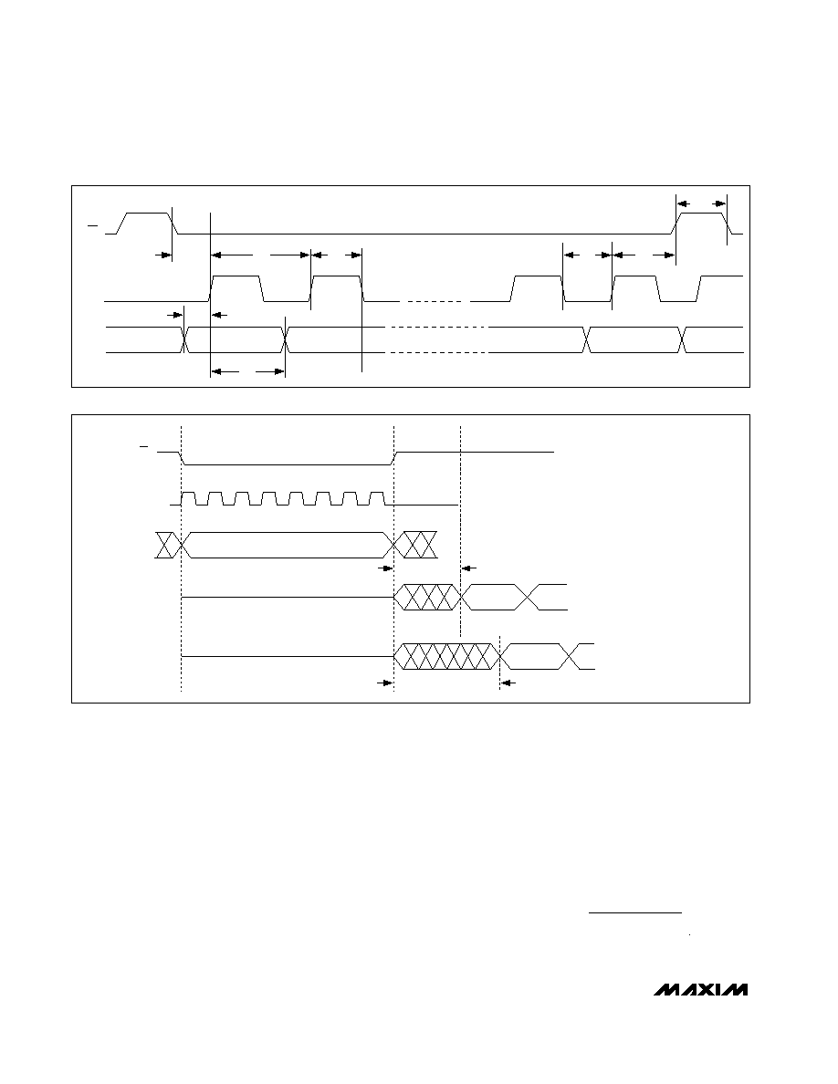
Mode Recovery Timing
Figure 6 shows the mode recovery timing diagram.
TWAKE is the wake-up time when exiting shutdown, idle,
or standby mode and entering into Rx, Tx, or Xcvr
mode. tENABLE is the recovery time when switching
between any Rx, Tx, or Xcvr mode. tWAKE or tENABLE is
the time for the ADC to settle within 1dB of specified
SINAD performance and DAC settling to 10 LSB error.
tWAKE or tENABLE times are measured after the 8-bit
serial command is latched into the MAX5864 by CS
transition high. tENABLE for Xcvr mode is dominated by
the DAC wake-up time. The recovery time is 10s to
switch between Xcvr, Tx, or Rx modes. The recovery
time is 40s to switch from shutdown or standby mode
to Xcvr mode.
System Clock Input (CLK)
CLK input is shared by both the ADCs and DACs. It
accepts a CMOS-compatible signal level set by OVDD
from 1.8V to VDD. Since the interstage conversion of the
device depends on the repeatability of the rising and
falling edges of the external clock, use a clock with low
jitter and fast rise and fall times (<2ns). Specifically,
sampling occurs on the rising edge of the clock signal,
requiring this edge to provide the lowest possible jitter.
Any significant clock jitter limits the SNR performance
of the on-chip ADCs as follows:
where fIN represents the analog input frequency and
tAJ is the time of the clock jitter.
SNR
tt
IN
AJ
=×
××
×
20
1
2
log
π
Ultra-Low-Power, High Dynamic-
Performance, 22Msps Analog Front End
18
______________________________________________________________________________________
Figure 5. 3-Wire Serial Interface Timing Diagram
MSB
CS
SCLK
DIN
LSB
tCSW
tCS
tCP
tCSS
tCL
tCH
tDS
tDH
Figure 6. MAX5864 Mode Recovery Timing Diagram
CS
SCLK
DIN
ID/QD
DAO–DA7
8-BIT DATA
ADC DIGITAL OUTPUT.
SINAD SETTLES WITHIN 1dB
DAC ANALOG OUTPUT. OUTPUT
SETTLES TO 10 LSB ERROR
tWAKE, SD, ST_ (Rx) OR tENABLE, Rx
tWAKE, SD, ST_ (Tx) OR tENABLE, TX
相关PDF资料 |
PDF描述 |
|---|---|
| MAX19711ETN+ | IC ANLG FRONT END 11MSPS 56-TQFN |
| V300C2M50BF3 | CONVERTER MOD DC/DC 2V 50W |
| MAX9140EXK+T | IC COMPARATOR R-R SC70-5 |
| V300C2M50BF | CONVERTER MOD DC/DC 2V 50W |
| B37950K1104K072 | CAP CER 0.1UF 100V 10% X7R 1210 |
相关代理商/技术参数 |
参数描述 |
|---|---|
| MAX5864ETM+ | 功能描述:ADC / DAC多通道 10-Bit 2Ch 22Msps CODEC/AFE RoHS:否 制造商:Texas Instruments 转换速率: 分辨率:8 bit 接口类型:SPI 电压参考: 电源电压-最大:3.6 V 电源电压-最小:2 V 最大工作温度:+ 85 C 安装风格:SMD/SMT 封装 / 箱体:VQFN-40 |
| MAX5864ETM+T | 功能描述:ADC / DAC多通道 10-Bit 2Ch 22Msps CODEC/AFE RoHS:否 制造商:Texas Instruments 转换速率: 分辨率:8 bit 接口类型:SPI 电压参考: 电源电压-最大:3.6 V 电源电压-最小:2 V 最大工作温度:+ 85 C 安装风格:SMD/SMT 封装 / 箱体:VQFN-40 |
| MAX5864ETM-T | 功能描述:ADC / DAC多通道 RoHS:否 制造商:Texas Instruments 转换速率: 分辨率:8 bit 接口类型:SPI 电压参考: 电源电压-最大:3.6 V 电源电压-最小:2 V 最大工作温度:+ 85 C 安装风格:SMD/SMT 封装 / 箱体:VQFN-40 |
| MAX5865ETM | 功能描述:ADC / DAC多通道 RoHS:否 制造商:Texas Instruments 转换速率: 分辨率:8 bit 接口类型:SPI 电压参考: 电源电压-最大:3.6 V 电源电压-最小:2 V 最大工作温度:+ 85 C 安装风格:SMD/SMT 封装 / 箱体:VQFN-40 |
| MAX5865ETM+ | 功能描述:ADC / DAC多通道 10-Bit 2Ch 40Msps CODEC/AFE RoHS:否 制造商:Texas Instruments 转换速率: 分辨率:8 bit 接口类型:SPI 电压参考: 电源电压-最大:3.6 V 电源电压-最小:2 V 最大工作温度:+ 85 C 安装风格:SMD/SMT 封装 / 箱体:VQFN-40 |
发布紧急采购,3分钟左右您将得到回复。