- 您现在的位置:买卖IC网 > PDF目录2011 > MAX5865ETM+T (Maxim Integrated Products)IC ANLG FRONT END 40MSPS 48-TQFN PDF资料下载
参数资料
| 型号: | MAX5865ETM+T |
| 厂商: | Maxim Integrated Products |
| 文件页数: | 4/26页 |
| 文件大小: | 0K |
| 描述: | IC ANLG FRONT END 40MSPS 48-TQFN |
| 产品培训模块: | Lead (SnPb) Finish for COTS Obsolescence Mitigation Program |
| 标准包装: | 2,500 |
| 位数: | 10 |
| 通道数: | 4 |
| 功率(瓦特): | 2.10W |
| 电压 - 电源,模拟: | 2.7 V ~ 3.3 V |
| 电压 - 电源,数字: | 1.8 V ~ 3.3 V |
| 封装/外壳: | 48-WFQFN 裸露焊盘 |
| 供应商设备封装: | 48-TQFN-EP(7x7) |
| 包装: | 带卷 (TR) |
MAX5865
Ultra-Low-Power, High-Dynamic-
Performance, 40Msps Analog Front End
12
______________________________________________________________________________________
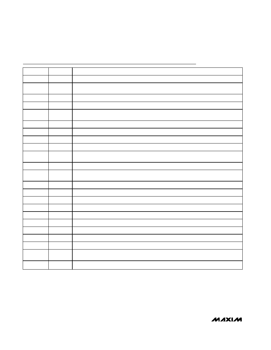
PIN
NAME
FUNCTION
1
REFP
Upper Reference Voltage. Bypass with a 0.33F capacitor to GND as close to REFP as possible.
2, 8, 43
VDD
Analog Supply Voltage. Bypass VDD to GND with a combination of a 2.2F capacitor in parallel with a
0.1F capacitor.
3
IA+
Channel IA Positive Analog Input. For single-ended operation, connect signal source to IA+.
4
IA-
Channel IA Negative Analog Input. For single-ended operation, connect IA- to COM.
5, 7, 12, 37,
42
GND
Analog Ground. Connect all pins to GND ground plane.
6
CLK
Conversion Clock Input. Clock signal for both ADCs and DACs.
9
QA-
Channel QA Negative Analog Input. For single-ended operation, connect QA- to COM.
10
QA+
Channel QA Positive Analog Input. For single-ended operation, connect signal source to QA+.
11, 33, 39
VDD
Analog Supply Voltage. Connect to VDD power plane as close to the device as possible.
13–16, 19–22
DA0–DA7
ADC Tri-State Digital Output Bits. DA7 is the most significant bit (MSB), and DA0 is the least
significant bit (LSB).
17
OGND
Output Driver Ground
18
OVDD
Output Driver Power Supply. Supply range from +1.8V to VDD to accommodate most logic levels.
Bypass OVDD to OGND with a combination of a 2.2F capacitor in parallel with a 0.1F capacitor.
23–32
DD0–DD9
DAC Digital Input Bits. DD9 is the MSB, and DD0 is the LSB.
34
DIN
3-Wire Serial Interface Data Input. Data is latched on the rising edge of the SCLK.
35
SCLK
3-Wire Serial Interface Clock Input
36
CS
3-Wire Serial Interface Chip Select Input. Apply logic low enables the serial interface.
38
N.C.
No Connection
40, 41
QD+, QD-
DAC Channel-QD Differential Voltage Output
44, 45
ID-, ID+
DAC Channel-ID Differential Voltage Output
46
REFIN
Reference Input. Connect to VDD for internal reference.
47
COM
Common-Mode Voltage I/O. Bypass COM to GND with a 0.33F capacitor.
48
REFN
Negative Reference I/O. Conversion range is
±(VREFP - VREFN). Bypass REFN to GND with a 0.33F
capacitor.
—
EP
Exposed Paddle. Exposed paddle is internally connected to GND. Connect EP to the GND plane.
Pin Description
相关PDF资料 |
PDF描述 |
|---|---|
| MAX5866ETM+ | IC ANLG FRONT END 60MSPS 48-TQFN |
| MAX5873EGK+D | IC DAC 12BIT 200MSPS DUAL 68-QFN |
| MAX5874EGK+D | IC DAC 14BIT 200MSPS DUAL 68-QFN |
| MAX5875EGK+D | IC DAC 16BIT DUAL 200MSPS 68-QFN |
| MAX5876EGK+D | IC DAC 12BIT DUAL 250MSPS 68-QFN |
相关代理商/技术参数 |
参数描述 |
|---|---|
| MAX5865EVKIT | 功能描述:数据转换 IC 开发工具 Evaluation Kit for the MAX5863 MAX5864 MAX5865 RoHS:否 制造商:Texas Instruments 产品:Demonstration Kits 类型:ADC 工具用于评估:ADS130E08 接口类型:SPI 工作电源电压:- 6 V to + 6 V |
| MAX5866ETM | 功能描述:ADC / DAC多通道 RoHS:否 制造商:Texas Instruments 转换速率: 分辨率:8 bit 接口类型:SPI 电压参考: 电源电压-最大:3.6 V 电源电压-最小:2 V 最大工作温度:+ 85 C 安装风格:SMD/SMT 封装 / 箱体:VQFN-40 |
| MAX5866ETM+ | 功能描述:ADC / DAC多通道 10-Bit 2Ch 60Msps CODEC/AFE RoHS:否 制造商:Texas Instruments 转换速率: 分辨率:8 bit 接口类型:SPI 电压参考: 电源电压-最大:3.6 V 电源电压-最小:2 V 最大工作温度:+ 85 C 安装风格:SMD/SMT 封装 / 箱体:VQFN-40 |
| MAX5866ETM+T | 功能描述:ADC / DAC多通道 10-Bit 2Ch 60Msps CODEC/AFE RoHS:否 制造商:Texas Instruments 转换速率: 分辨率:8 bit 接口类型:SPI 电压参考: 电源电压-最大:3.6 V 电源电压-最小:2 V 最大工作温度:+ 85 C 安装风格:SMD/SMT 封装 / 箱体:VQFN-40 |
| MAX5866ETM-T | 功能描述:ADC / DAC多通道 RoHS:否 制造商:Texas Instruments 转换速率: 分辨率:8 bit 接口类型:SPI 电压参考: 电源电压-最大:3.6 V 电源电压-最小:2 V 最大工作温度:+ 85 C 安装风格:SMD/SMT 封装 / 箱体:VQFN-40 |
发布紧急采购,3分钟左右您将得到回复。