- 您现在的位置:买卖IC网 > Datasheet目录43 > MAX5932ESA+T (Maxim Integrated)IC HOT-SWAP CONTROLLER 8-SOIC Datasheet资料下载
参数资料
| 型号: | MAX5932ESA+T |
| 厂商: | Maxim Integrated |
| 文件页数: | 2/15页 |
| 文件大小: | 247K |
| 描述: | IC HOT-SWAP CONTROLLER 8-SOIC |
| 产品培训模块: | Lead (SnPb) Finish for COTS Obsolescence Mitigation Program |
| 标准包装: | 2,500 |
| 类型: | 热交换控制器 |
| 应用: | 通用 |
| 内部开关: | 无 |
| 电源电压: | 9 V ~ 80 V |
| 工作温度: | -40°C ~ 85°C |
| 安装类型: | 表面贴装 |
| 封装/外壳: | 8-SOIC(0.154",3.90mm 宽) |
| 供应商设备封装: | 8-SOIC |
| 包装: | 带卷 (TR) |
Positive High-Voltage, Hot-Swap Controller
2 _______________________________________________________________________________________
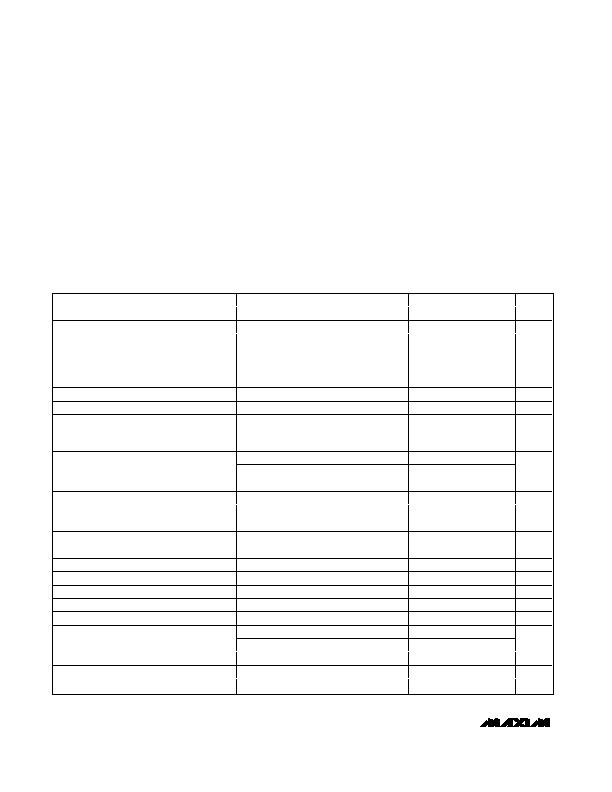
ABSOLUTE MAXIMUM RATINGS
ELECTRICAL CHARACTERISTICS
(V
CC
= +24V, GND = 0V, T
A
= -40癈 to +85癈, unless otherwise noted. Typical values are at T
A
= +25癈.) (Note 1)
Stresses beyond those listed under
Absolute Maximum Ratings
may cause permanent damage to the device. These are stress ratings only, and functional
operation of the device at these or any other conditions beyond those indicated in the operational sections of the specifications is not implied. Exposure to
absolute maximum rating conditions for extended periods may affect device reliability.
(Voltages referenced to GND)
V
CC
.........................................................................-0.3V to +85V
SENSE, FB, ON ..........................................-0.3V to (V
CC
+ 0.3V)
TIMER, PWRGD......................................................-0.3V to +85V
GATE ......................................................................-0.3V to +95V
Maximum GATE Current ....................................-50mA, +150mA
Maximum Current into Any Other Pin................................?0mA
Continuous Power Dissipation (T
A
= +70癈)
8-Pin SO (derate 5.9mW/癈 above +70癈)..................470mW
Operating Temperature Range ...........................-40癈 to +85癈
Maximum Junction Temperature .....................................+150癈
Storage Temperature Range.............................-60癈 to +150癈
ESD Rating (Human Body Model)......................................2000V
Lead Temperature (soldering, 10s).................................+300癈
PARAMETER
SYMBOL
CONDITIONS
MIN
TYP
MAX
UNITS
Supply Voltage Range
V
CC
9
80
V
Supply Current
I
CC
V
ON
= 3V, V
CC
= 80V
1.4
3.5
mA
V
CC
Undervoltage Lockout
V
LKO
V
CC
low-to-high transition
7.5
8.3
8.8
V
V
CC
Undervoltage Lockout
Hysteresis
V
LKOHYST
0.4
V
FB High-Voltage Threshold
V
FBH
FB low-to-high transition
1.280
1.313
1.345
V
FB Low-Voltage Threshold
V
FBL
FB high-to-low transition
1.221
1.233
1.245
V
FB Hysteresis
V
FBHYST
80
mV
FB Input Bias Current
I
INFB
V
FB
= 0V
-1
+1
礎
FB Threshold Line Regulation
V
FB
9V d V
CC
d 80V, ON = 0V,
T
A
= 0癈 to +70癈
0.05
mV/V
V
FB
= 0V, T
A
= 0癈 to +70癈
8
12
17
SENSE Trip Voltage
(V
CC
- V
SENSE
)
V
SENSETRIP
V
FB
= 1V, T
A
= 0癈 to +70癈
39
47
55
mV
GATE Pullup Current
I
GATEUP
Charge pump on, V
GATE
= 7V
-5
-10
-20
礎
GATE Pulldown Current
I
GATEDN
Any fault condition, V
GATE
= 2V
35
70
100
mA
V
CC
= 10.8V to 20V
4.5
6.2
18
External N-Channel Gate Drive
V
GATE
V
GATE
- V
CC
V
CC
= 20V to 80V
10
13.6
18
V
TIMER Pullup Current
I
TIMERUP
V
TIMER
= 0V
-24
-80
-120
礎
TIMER Pulldown Current
I
TIMERON
V
TIMER
= 1V
1.5
3
4.5
礎
ON Logic-High Threshold
V
ONH
ON low-to-high transition
1.280
1.313
1.355
V
ON Logic-Low Threshold
V
ONL
ON high-to-low transition
1.221
1.233
1.245
V
ON Hysteresis
V
ONHYST
80
mV
ON Input Bias Current
I
INON
V
ON
= 0V
-1
+1
礎
PWRGD Leakage Current
I
OH
V
PWRGD
= 80V
10
礎
I
O
= 2mA
0.4
PWRGD Output Low Voltage
V
OL
I
O
= 4mA
2.5
V
SENSE Input Bias Current
I
SENSE
V
SENSE
= 0V to V
CC
-1
+3
礎
Thermal Shutdown
Temperature rising
150
癈
Thermal Shutdown Hysteresis
20
癈
相关PDF资料 |
PDF描述 |
|---|---|
| MAX5933EESA+ | IC HOT-SWAP CONTROLLER 8-SOIC |
| MAX5934EEE+ | IC HOT-SWAP CONTROLLER 16-QSOP |
| MAX5935EAX+ | IC CTRLR POWER QUAD 36-SSOP |
| MAX5937LCESA+ | IC HOT-SWAP CTRLR -48V 8-SOIC |
| MAX5938LEEE+ | IC HOT-SWAP CTRLR -48V 16-QSOP |
相关代理商/技术参数 |
参数描述 |
|---|---|
| MAX5932ESA-TG077 | 功能描述:热插拔功率分布 RoHS:否 制造商:Texas Instruments 产品:Controllers & Switches 电流限制: 电源电压-最大:7 V 电源电压-最小:- 0.3 V 工作温度范围: 功率耗散: 安装风格:SMD/SMT 封装 / 箱体:MSOP-8 封装:Tube |
| MAX5932EVKIT | 功能描述:热插拔功率分布 Evaluation Kit for the MAX5932 RoHS:否 制造商:Texas Instruments 产品:Controllers & Switches 电流限制: 电源电压-最大:7 V 电源电压-最小:- 0.3 V 工作温度范围: 功率耗散: 安装风格:SMD/SMT 封装 / 箱体:MSOP-8 封装:Tube |
| MAX5933AESA | 功能描述:热插拔功率分布 RoHS:否 制造商:Texas Instruments 产品:Controllers & Switches 电流限制: 电源电压-最大:7 V 电源电压-最小:- 0.3 V 工作温度范围: 功率耗散: 安装风格:SMD/SMT 封装 / 箱体:MSOP-8 封装:Tube |
| MAX5933AESA+ | 功能描述:热插拔功率分布 Positive Hot-Swap Controller RoHS:否 制造商:Texas Instruments 产品:Controllers & Switches 电流限制: 电源电压-最大:7 V 电源电压-最小:- 0.3 V 工作温度范围: 功率耗散: 安装风格:SMD/SMT 封装 / 箱体:MSOP-8 封装:Tube |
| MAX5933AESA+T | 功能描述:热插拔功率分布 Positive Hot-Swap Controller RoHS:否 制造商:Texas Instruments 产品:Controllers & Switches 电流限制: 电源电压-最大:7 V 电源电压-最小:- 0.3 V 工作温度范围: 功率耗散: 安装风格:SMD/SMT 封装 / 箱体:MSOP-8 封装:Tube |
发布紧急采购,3分钟左右您将得到回复。