- 您现在的位置:买卖IC网 > PDF目录20027 > MAX5949AESA+ (Maxim Integrated)IC HOT SWAP CONTROL 8-SOIC PDF资料下载
参数资料
| 型号: | MAX5949AESA+ |
| 厂商: | Maxim Integrated |
| 文件页数: | 10/18页 |
| 文件大小: | 186K |
| 描述: | IC HOT SWAP CONTROL 8-SOIC |
| 产品培训模块: | Lead (SnPb) Finish for COTS Obsolescence Mitigation Program |
| 标准包装: | 100 |
| 类型: | 热交换控制器 |
| 应用: | 通用 |
| 内部开关: | 无 |
| 电源电压: | -20 V ~ -80 V |
| 工作温度: | -40°C ~ 85°C |
| 安装类型: | 表面贴装 |
| 封装/外壳: | 8-SOIC(0.154",3.90mm 宽) |
| 供应商设备封装: | 8-SOIC |
| 包装: | 管件 |
| 产品目录页面: | 1423 (CN2011-ZH PDF) |
In either case, when the MOSFET is turned off, the out-
put capacitor continues to discharge by the IC supply
current, I
DD
. The I
DD
flows into the IC at the V
DD
termi-
nal, out at the V
EE
terminal, and back to the capacitor
through the external MOSFETs substrate diode. There
is also a parallel current path between the V
EE
and
DRAIN terminals through multiple internal ESD-protec-
tion diodes. Protection circuits built into the IC allow the
DRAIN terminal voltage to drop below that of the V
EE
terminal so long as the allowed absolute-maximum
DRAIN terminal current (-100mA) is not exceeded. As
I
DD
is only 2mA maximum, this limiting current will not
even be approached.
Current Limit and Electronic
Circuit Breaker
The MAX5949_ provides current-limiting and circuit-
breaker features that protect against excessive load cur-
rent and short-circuit conditions. The load current is
monitored by sensing the voltage across an external
sense resistor connected between V
EE
and SENSE.
If the voltage between V
EE
and SENSE reaches the cur-
rent-limit trip voltage (V
CL
), the MAX5949_ pulls down
the GATE pin and regulates the current through the
external MOSFET so V
SENSE
- V
EE
<
V
CL
. If the current
drawn by the load drops below V
CL
/ R
SENSE
limit, the
GATE pin voltage rises again. However, if the load cur-
rent is at the regulation limit of V
CL
/ R
SENSE
for a period
of t
PHLCB
, the electronic circuit breaker trips, causing the
MAX5949A/MAX5949B to turn off the external MOSFET.
After an overcurrent fault condition, the circuit breaker
is reset by pulling the UV pin low and then pulling UV
high or by cycling power to the MAX5949A/MAX5949B.
Unless power is cycled to the MAX5949A/MAX5949B,
the device waits until t
OFF
has elapsed before turning
on the gate of the external FET.
Overcurrent Fault Integrator
The MAX5949_ features an overcurrent fault integrator.
When an overcurrent condition exists, an internal digital
counter increments its count. When the counter reaches
500祍 (the maximum current-limit duration) for the
MAX5949_, an overcurrent fault is generated. If the
overcurrent fault does not last 500祍, then the counter
begins decrementing at a rate 128 (maximum current-
limit duty cycle) times slower than the counter was
incrementing. Repeated overcurrent conditions will gen-
erate a fault if duty cycle of the overcurrent condition is
greater than 1/128.
Load-Current Regulation
The MAX5949_ accomplishes load-current regulation by
pulling current from the GATE pin whenever V
SENSE
- V
EE
> V
CL
(see the Typical Operating Characteristics). This
decreases the gate-to-source voltage of the external
MOSFET, thereby reducing the load current. When
V
SENSE
- V
EE
< V
CL
, the MAX5949A/MAX5949B pull the
GATE pin high by a 45礎 (I
PU
) current.
Driving into a Shorted Load
In the event of a permanent short-circuit condition, the
MAX5949_ limits the current drawn by the load to V
CL
/
R
SENSE
for a period of t
PHLCB
, after which the circuit
breaker trips. Once the circuit breaker trips, the GATE
of the external FET is pulled low by 50mA (I
PD
) turning
off power to the load.
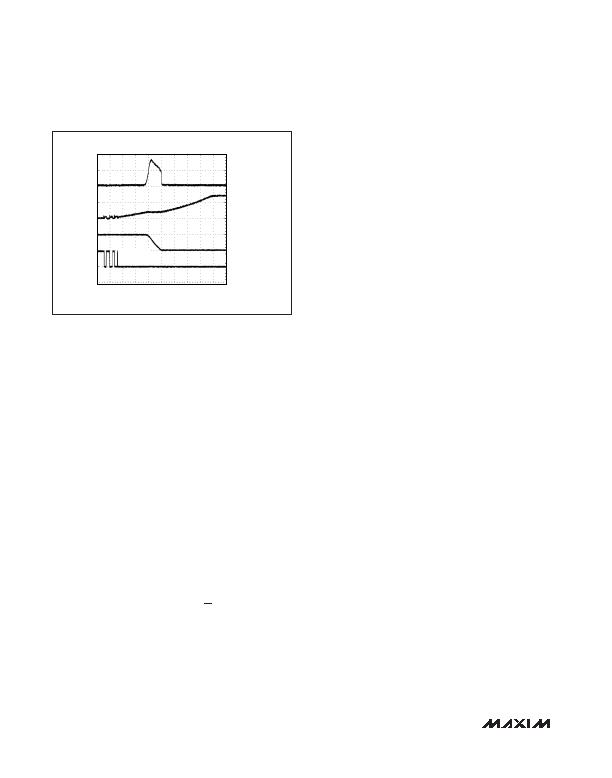
Immunity to Input Voltage Steps
The MAX5949_ guards against input voltage steps on the
input supply. A rapid increase in the input supply voltage
(V
DD
- V
EE
increasing) causes a current step equal to I =
C
L
x V
IN
/ T. If the load current exceeds V
CL
/ R
SENSE
during an input voltage step, the MAX5949A/MAX5949B
current limit activates, pulling down the gate voltage and
limiting the load current to V
CL
/ R
SENSE
. The DRAIN
voltage (V
DRAIN
) then slews at a slower rate than the
input voltage. As the drain voltage starts to slew down,
the drain-to-gate feedback capacitor C2 pushes back on
the gate, reducing the gate-to-source voltage (V
GS
) and
the current through the external MOSFET. Once the input
supply reaches its final value, the DRAIN slew rate (and
therefore the inrush current) is limited by the capacitor
C2 just as it is limited in the startup condition. To ensure
correct operation, R
SENSE
must be chosen to provide a
current limit larger than the sum of the load current and
the dynamic current into the load capacitance in the
slewing mode.
If the load current plus the capacitive charging current is
-48V Hot-Swap Controllers
with External R
SENSE
10 ______________________________________________________________________________________
GATE - V
EE
10V/div
V
EE
50V/div
DRAIN
50V/div
INRUSH
CURRENT
1A/div
4ms/div
CONTACT
BOUNCE
Figure 7b. Input Inrush Current
相关PDF资料 |
PDF描述 |
|---|---|
| VE-JTY-CX-B1 | CONVERTER MOD DC/DC 3.3V 49.5W |
| NCV8502D100R2G | IC REG LDO 10V .15A 8SOIC |
| RMA35DTKS | CONN EDGECARD 70POS DIP .125 SLD |
| ISL6173DRZA | IC CTRLR HOT SWAP DUAL LV 28QFN |
| VY2150K29U2JS6TV7 | CAP CER 15PF 300V 10% RADIAL |
相关代理商/技术参数 |
参数描述 |
|---|---|
| MAX5949AESA+ | 功能描述:热插拔功率分布 48V- Hot-Swap Controller RoHS:否 制造商:Texas Instruments 产品:Controllers & Switches 电流限制: 电源电压-最大:7 V 电源电压-最小:- 0.3 V 工作温度范围: 功率耗散: 安装风格:SMD/SMT 封装 / 箱体:MSOP-8 封装:Tube |
| MAX5949AESA+T | 功能描述:热插拔功率分布 48V- Hot-Swap Controller RoHS:否 制造商:Texas Instruments 产品:Controllers & Switches 电流限制: 电源电压-最大:7 V 电源电压-最小:- 0.3 V 工作温度范围: 功率耗散: 安装风格:SMD/SMT 封装 / 箱体:MSOP-8 封装:Tube |
| MAX5949AESA+TG126 | 制造商:Rochester Electronics LLC 功能描述: 制造商:Maxim Integrated Products 功能描述: |
| MAX5949AESA-T | 功能描述:热插拔功率分布 RoHS:否 制造商:Texas Instruments 产品:Controllers & Switches 电流限制: 电源电压-最大:7 V 电源电压-最小:- 0.3 V 工作温度范围: 功率耗散: 安装风格:SMD/SMT 封装 / 箱体:MSOP-8 封装:Tube |
| MAX5949BESA | 功能描述:热插拔功率分布 RoHS:否 制造商:Texas Instruments 产品:Controllers & Switches 电流限制: 电源电压-最大:7 V 电源电压-最小:- 0.3 V 工作温度范围: 功率耗散: 安装风格:SMD/SMT 封装 / 箱体:MSOP-8 封装:Tube |
发布紧急采购,3分钟左右您将得到回复。