- 您现在的位置:买卖IC网 > PDF目录1844 > MAX629ESA-T (Maxim Integrated Products)IC REG MULTI CONFIG +/-28V 8SOIC PDF资料下载
参数资料
| 型号: | MAX629ESA-T |
| 厂商: | Maxim Integrated Products |
| 文件页数: | 5/12页 |
| 文件大小: | 0K |
| 描述: | IC REG MULTI CONFIG +/-28V 8SOIC |
| 产品培训模块: | Lead (SnPb) Finish for COTS Obsolescence Mitigation Program |
| 标准包装: | 2,500 |
| 类型: | 升压(升压),反相,回扫,Sepic |
| 输出类型: | 固定 |
| 输出数: | 1 |
| 输出电压: | ±28V |
| 输入电压: | 2.7 V ~ 5.5 V |
| 频率 - 开关: | 300kHz |
| 电流 - 输出: | 500mA |
| 同步整流器: | 无 |
| 工作温度: | -40°C ~ 85°C |
| 安装类型: | 表面贴装 |
| 封装/外壳: | 8-SOIC(0.154",3.90mm 宽) |
| 包装: | 带卷 (TR) |
| 供应商设备封装: | 8-SOIC |
�� �
�
�28V,� Low-Power,� High-Voltage,�
�Boost� or� Inverting� DC-DC� Converter�
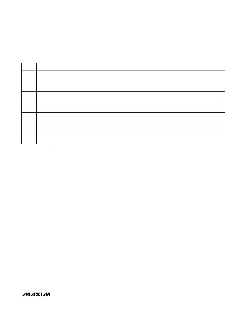
�______________________________________________________________Pin� Description�
�PIN�
�1�
�2�
�3�
�4�
�5�
�6�
�7�
�8�
�NAME�
�SHDN�
�POL�
�REF�
�FB�
�ISET�
�GND�
�LX�
�V� CC�
�FUNCTION�
�Active-Low� Shutdown� Input.� A� logic� low� puts� the� MAX629� in� shutdown� mode� and� reduces� supply� current� to�
�1μA.�
�Polarity� Input.� Changes� polarity� and� threshold� of� FB� to� allow� regulation� of� either� positive� or� negative� output�
�voltages.� Set� POL� =� GND� for� positive� output� voltage,� or� set� POL� =� V� CC� for� negative� output� voltage.�
�1.25V� Reference� Output.� Bypass� to� GND� with� a� 0.1μF� capacitor� for� I� REF� ≤� 10μA.� REF� can� source� 100μA� to�
�drive� external� loads.� For� 10μA� ≤� I� REF� ≤� 100μA,� bypass� REF� with� a� 0.47μF� capacitor.�
�Feedback� Input� for� setting� output� voltage.� Connect� to� an� external� voltage� divider.� See� Setting� the� Output�
�Voltage.�
�Current-Limit� Set� Input.� Connect� to� V� CC� for� a� 500mA� LX� current� limit,� or� connect� to� GND� for� a� 250mA� LX�
�current� limit.� See� Setting� the� Current� Limit.�
�Ground�
�Internal� N-Channel� DMOS� Switch� Drain�
�Power-Supply� Input�
�_______________Detailed� Description�
�The� MAX629� low-power,� boost� DC-DC� converter� pro-�
�vides� either� positive� or� negative� output� voltages� up� to�
�±28V� from� a� wide� range� of� input� voltages.� It� is�
�designed� primarily� for� use� in� low-power,� high-voltage�
�applications� such� as� LCD� biasing� and� set-top� box� var-�
�actor� tuning.� The� MAX629� ’s� unique� control� scheme�
�provides� high� efficiency� and� a� wide� range� of� output�
�voltages� with� only� 80μA� quiescent� supply� current,� mak-�
�ing� it� ideal� for� battery-powered� applications.� The� inter-�
�nal� N-channel� DMOS� switch� has� a� pin-programmable�
�current� limit� (250mA� and� 500mA),� allowing� optimization�
�of� output� current� and� component� size.� Figure� 1� shows�
�the� MAX629� functional� diagram.�
�Control� Scheme�
�A� combination� of� peak-current� limiting� and� a� pair� of�
�one-shots� controls� the� MAX629� switching,� determining�
�the� maximum� on-time� and� constant� off-time.� During� the�
�on-cycle,� the� internal� switch� closes,� and� current�
�through� the� inductor� ramps� up� until� either� the� fixed�
�10μs� maximum� on-time� expires� (at� low� input� voltages)�
�or� the� switch’s� peak� current� limit� is� reached.� The� peak�
�switch� current� limit� is� selectable� to� either� 500mA� (ISET�
�=� V� CC� )� or� 250mA� (ISET� =� GND)� (see� Setting� the�
�Current� Limit).� After� the� on-cycle� terminates,� the� switch�
�turns� off,� charging� the� output� capacitor� through� the�
�diode.� In� normal� operation,� the� minimum� off-time� is� set�
�to� 1μs� for� positive� output� voltages� and� 3.5μs� for� nega-�
�tive� output� voltages.� When� the� output� is� well� below� reg-�
�ulation,� however,� the� off-time� is� increased� to� 5μs� to� pro-�
�vide� soft-start� during� start-up.� The� switching� frequency,�
�which� depends� upon� the� load,� can� be� as� high� as�
�300kHz.�
�Shutdown� Mode�
�When� SHDN� is� low,� the� MAX629� enters� shutdown�
�mode.� In� this� mode,� the� feedback� and� control� circuit,�
�reference,� and� internal� biasing� circuitry� turn� off.� The�
�shutdown� current� drops� to� less� than� 1μA.� SHDN� is� a�
�logic-level� input;� connect� it� to� V� CC� for� normal� operation.�
�The� output� voltage� behavior� in� shutdown� mode�
�depends� on� the� output� voltage� polarity.� In� the� positive�
�output� voltage� configuration� (Figure� 2),� the� output� is�
�directly� connected� to� the� input� through� the� diode� (D1)�
�and� the� inductor� (L1).� When� the� device� is� in� shutdown�
�mode,� the� output� voltage� falls� to� one� diode� drop� below�
�the� input� voltage,� and� any� load� connected� to� the� output�
�may� still� conduct� current.� In� the� negative� output� voltage�
�configuration� (Figure� 3),� there� is� no� DC� connection�
�between� the� input� and� the� output,� and� in� shutdown�
�mode� the� output� is� pulled� to� GND.�
�__________________Design� Procedure�
�Setting� the� Output� Voltage�
�For� either� positive� or� negative� output� voltage� applica-�
�tions,� set� the� MAX629’s� output� voltage� using� two� exter-�
�nal� resistors,� R1� and� R2,� as� shown� in� Figures� 2� and� 3.�
�Since� the� input� bias� current� at� FB� has� a� 50nA� maximum�
�value,� large� resistors� can� be� used� in� the� feedback� loop�
�_______________________________________________________________________________________�
�5�
�相关PDF资料 |
PDF描述 |
|---|---|
| MAX6304ESA | IC CIRCUIT SUPERVISORY LP 8-SOIC |
| MAX6306UK31D3-T | IC PROGRAM 3.080V RESET SOT23-5 |
| MAX6314US41D3+T | IC RESET CIRCUIT 4.10V SOT143-4 |
| MAX6315US29D2-T | IC RESET CIRCUIT 2.93V SOT143-4 |
| MAX631ACSA | IC REG BOOST 5V/ADJ 50MA 8SOIC |
相关代理商/技术参数 |
参数描述 |
|---|---|
| MAX629ESA-TG068 | 制造商:Maxim Integrated Products 功能描述:28V, LOW-POWER, HIGH-VOLTAGE BOOST OR INVERTI - Tape and Reel |
| MAX629EVKIT | 功能描述:直流/直流开关转换器 Evaluation Kit for the MAX629 RoHS:否 制造商:STMicroelectronics 最大输入电压:4.5 V 开关频率:1.5 MHz 输出电压:4.6 V 输出电流:250 mA 输出端数量:2 最大工作温度:+ 85 C 安装风格:SMD/SMT |
| MAX63___R | 制造商:MAXIM 制造商全称:Maxim Integrated Products 功能描述:Dual/Triple-Voltage ??P Supervisory Circuits |
| MAX63___S | 制造商:MAXIM 制造商全称:Maxim Integrated Products 功能描述:Dual/Triple-Voltage ??P Supervisory Circuits |
| MAX63___T | 制造商:MAXIM 制造商全称:Maxim Integrated Products 功能描述:Dual/Triple-Voltage ??P Supervisory Circuits |
发布紧急采购,3分钟左右您将得到回复。