- 您现在的位置:买卖IC网 > PDF目录1844 > MAX629ESA-T (Maxim Integrated Products)IC REG MULTI CONFIG +/-28V 8SOIC PDF资料下载
参数资料
| 型号: | MAX629ESA-T |
| 厂商: | Maxim Integrated Products |
| 文件页数: | 9/12页 |
| 文件大小: | 0K |
| 描述: | IC REG MULTI CONFIG +/-28V 8SOIC |
| 产品培训模块: | Lead (SnPb) Finish for COTS Obsolescence Mitigation Program |
| 标准包装: | 2,500 |
| 类型: | 升压(升压),反相,回扫,Sepic |
| 输出类型: | 固定 |
| 输出数: | 1 |
| 输出电压: | ±28V |
| 输入电压: | 2.7 V ~ 5.5 V |
| 频率 - 开关: | 300kHz |
| 电流 - 输出: | 500mA |
| 同步整流器: | 无 |
| 工作温度: | -40°C ~ 85°C |
| 安装类型: | 表面贴装 |
| 封装/外壳: | 8-SOIC(0.154",3.90mm 宽) |
| 包装: | 带卷 (TR) |
| 供应商设备封装: | 8-SOIC |
�� �
�
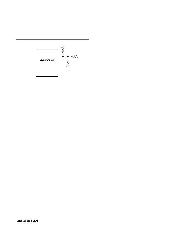
�28V,� Low-Power,� High-Voltage,�
�Boost� or� Inverting� DC-DC� Converter�
�V� OUT�
�R1�
�R� B�
�limit� threshold.� Resistor� R3� increases� the� usable� input�
�voltage� range� by� limiting� the� peak� injected� current.� The�
�2� ?� resistor� shown� provides� a� usable� input� voltage�
�range� beyond� V� IN� =� 15V.� In� applications� with� a� different�
�input� voltage� range,� R3� may� be� increased� or�
�FB�
�MAX629�
�GND�
�(REF)�
�(� )� ARE� FOR� NEGATIVE� OUTPUT� VOLTAGE� CONFIGURATIONS.�
�Figure� 4.� Adjustable� Output� Voltage�
�R2�
�V� BIAS�
�decreased� as� necessary,� with� a� resulting� efficiency�
�change� of� roughly� 0.5%/� ?� .�
�Layout� Considerations�
�Proper� PC� board� layout� is� essential� due� to� high� current�
�levels� and� fast� switching� waveforms� that� radiate� noise.�
�It� is� recommended� that� initial� prototyping� be� performed�
�using� the� MAX629� evaluation� kit� or� equivalent� PC�
�board-based� design.� Breadboards� or� proto-boards�
�should� never� be� used� when� prototyping� switching� reg-�
�ulators.�
�increasing� usable� battery� life.� Using� separate� supplies�
�for� V� CC� and� V� IN� also� reduces� noise� injection� onto� V� CC�
�by� isolating� it� from� the� switching� transients,� allowing� a�
�smaller,� less-expensive� input� filter� capacitor� to� be� used�
�in� many� applications.� If� input� voltages� below� 2V� will� be�
�common,� reducing� the� inductor� to� 22μH� may� improve�
�performance� in� this� voltage� range,� at� the� potential� cost�
�of� some� decrease� in� maximum� load� current� and� effi-�
�ciency.�
�In� the� negative� configuration� shown� in� Figure� 3,� the�
�inverting� charge� pump� injects� current� into� LX� with� each�
�cycle.� The� amount� of� charge� injected� increases� at�
�higher� V� IN� ,� and� may� prematurely� trip� the� internal� current-�
�It� is� important� to� connect� the� GND� pin,� the� input�
�bypass-capacitor� ground� lead,� and� the� output� filter-�
�capacitor� ground� lead� to� a� single� point� (star� ground�
�configuration)� to� minimize� ground� noise� and� improve�
�regulation.� Also,� minimize� lead� lengths� to� reduce� stray�
�capacitance,� trace� resistance,� and� radiated� noise,� with�
�preference� given� to� the� feedback� circuit,� the� ground�
�circuit,� and� LX.� Place� R1� and� R2� as� close� to� the� feed-�
�back� pin� as� possible.� Place� the� input� bypass� capacitor�
�as� close� as� possible� to� V� CC� and� GND.�
�Refer� to� the� MAX629� evaluation� kit� data� sheet� for� an�
�example� of� proper� board� layout.�
�_______________________________________________________________________________________�
�9�
�相关PDF资料 |
PDF描述 |
|---|---|
| MAX6304ESA | IC CIRCUIT SUPERVISORY LP 8-SOIC |
| MAX6306UK31D3-T | IC PROGRAM 3.080V RESET SOT23-5 |
| MAX6314US41D3+T | IC RESET CIRCUIT 4.10V SOT143-4 |
| MAX6315US29D2-T | IC RESET CIRCUIT 2.93V SOT143-4 |
| MAX631ACSA | IC REG BOOST 5V/ADJ 50MA 8SOIC |
相关代理商/技术参数 |
参数描述 |
|---|---|
| MAX629ESA-TG068 | 制造商:Maxim Integrated Products 功能描述:28V, LOW-POWER, HIGH-VOLTAGE BOOST OR INVERTI - Tape and Reel |
| MAX629EVKIT | 功能描述:直流/直流开关转换器 Evaluation Kit for the MAX629 RoHS:否 制造商:STMicroelectronics 最大输入电压:4.5 V 开关频率:1.5 MHz 输出电压:4.6 V 输出电流:250 mA 输出端数量:2 最大工作温度:+ 85 C 安装风格:SMD/SMT |
| MAX63___R | 制造商:MAXIM 制造商全称:Maxim Integrated Products 功能描述:Dual/Triple-Voltage ??P Supervisory Circuits |
| MAX63___S | 制造商:MAXIM 制造商全称:Maxim Integrated Products 功能描述:Dual/Triple-Voltage ??P Supervisory Circuits |
| MAX63___T | 制造商:MAXIM 制造商全称:Maxim Integrated Products 功能描述:Dual/Triple-Voltage ??P Supervisory Circuits |
发布紧急采购,3分钟左右您将得到回复。