- 您现在的位置:买卖IC网 > PDF目录69018 > MAX6917EO33 (MAXIM INTEGRATED PRODUCTS INC) REAL TIME CLOCK, PDSO20 PDF资料下载
参数资料
| 型号: | MAX6917EO33 |
| 厂商: | MAXIM INTEGRATED PRODUCTS INC |
| 元件分类: | 时钟/数据恢复及定时提取 |
| 英文描述: | REAL TIME CLOCK, PDSO20 |
| 封装: | 0.150 INCH, 0.025 INCH PITCH, MO-137AD, QSOP-20 |
| 文件页数: | 3/31页 |
| 文件大小: | 349K |
| 代理商: | MAX6917EO33 |
第1页第2页当前第3页第4页第5页第6页第7页第8页第9页第10页第11页第12页第13页第14页第15页第16页第17页第18页第19页第20页第21页第22页第23页第24页第25页第26页第27页第28页第29页第30页第31页
MAX6917
I2C-Compatible RTC with Microprocessor
Supervisor, Alarm, and NV RAM Controller
______________________________________________________________________________________
11
Detailed Description
Functional Description
The MAX6917 contains eight 8-bit timekeeping registers,
seven 8-bit alarm threshold registers, one status register,
one control register, one alarm-configuration register, and
96 x 8 bits of SRAM. In addition to single-byte reads and
writes to registers and RAM, there is a burst timekeeping
register read/write command, a burst RAM read/write
command, and a battery-test command that allows soft-
ware-commanded testing of the backup battery at any
time. An I2C-bus-compatible interface allows serial com-
munication with a P. When VCC is less than the reset
threshold, the serial interface is disabled to prevent erro-
neous data from being written to the MAX6917. A P
supervisory section and an NVRAM controller are provid-
ed for ease of implementation with P-based systems. A
crystal fail-detect circuit and a data-valid bit can be used
to guarantee RAM data integrity and valid timekeeping
data. Two reference frequencies outputs, 32.768kHz and
1Hz, are provided for external device clocking. Time and
calendar data are stored in a binary-coded decimal
(BCD) format. Figure 1 shows the functional diagram of
the MAX6917.
Real-Time Clock
The RTC provides seconds, minutes, hours, day, date,
month, and year information. The end of the months is
automatically adjusted for months with fewer than 31
days, including corrections for leap years through 2099.
Crystal Oscillator
The MAX6917 uses an external, standard 6pF load
watch crystal. No other external components are
required for this timekeeping oscillator. Power-up oscil-
lator start time is dependent mainly upon applied VCC
and ambient temperature. The MAX6917, because of
its low timekeeping current, exhibits a typical startup
time of 1s to 2s.
I2C-Compatible Interface
The I2C bus allows bidirectional, 2-wire communication
between different ICs. The two lines are serial data line
(SDA) and serial clock line (SCL). Both lines must be
connected to a positive supply through individual
pullup resistors (see the Typical Application Circuit).
Data transfer can only be initiated when the bus is not
busy (both SDA and SCL are high). Figure 2 shows a
timing diagram for I2C communication.
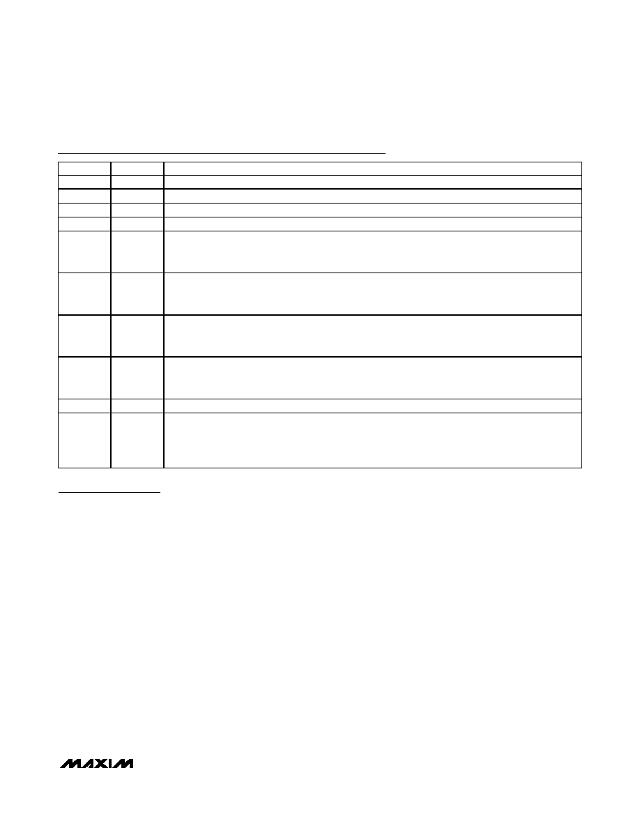
Pin Description (continued)
PIN
NAME
FUNCTION
11
32KHZ
32.768kHz Output. Buffered push-pull output that is enabled from the FOUT configuration register.
12
1HZ
1Hz Output. Buffered push-pull output that is enabled from the FOUT configuration register.
13
SDA
Open-Drain Data Input/Output. I2C bus serial data input/output connection.
14
SCL
Serial Clock Input. I2C bus clock for input/output data transfers.
15
ALM
Open-Drain, Active-Low Alarm Output. ALM goes low when RTC time matches alarm thresholds set in
the alarm threshold registers. ALM stays low until cleared by reading or writing to the alarm configuration
register or to any of the alarm threshold registers.
16
CE_OUT
Chip-Enable Output. CE_OUT goes low only when CE_IN is low and RESET is not asserted. If CE_IN is
low when RESET is asserted, CE_OUT remains low for tRCE or until CE_IN goes high, whichever occurs
first. CE_OUT is pulled to VOUT.
17
BATT_LO
Open-Drain, Battery-Low Indicator. BATT_LO is active low when the VBATT input is tested below VBTP if
the internal trip is selected in the control register (POR default). If external trip is selected in the control
register, then BATT_LO is active low when TRIP is less than VTRIP.
18
RESET
Open-Drain, Active-Low Reset Output. RESET pulses low for tRP when triggered, and stays low
whenever VCC is below the reset threshold or when MR is logic low. RESET remains low for tRP after
either VCC rises above the reset threshold or MR goes from low to high.
19
VCC
Main Supply Input. Connect a 0.1F bypass capacitor from VCC to GND.
20
VBATT
Backup-Battery Input. When VCC falls below the reset threshold and VBATT, VOUT switches from VCC to
VBATT. When VCC rises above VBATT or the reset threshold, VOUT reconnects to VCC. VBATT may exceed
VCC. Connect VBATT to GND if no backup-battery supply is used. Connect a 0.1F low-leakage bypass
capacitor from VBATT to GND.
相关PDF资料 |
PDF描述 |
|---|---|
| MAX8893AEWV+ | SPECIALTY MICROPROCESSOR CIRCUIT, PBGA30 |
| MAX8893BEWV+ | SPECIALTY MICROPROCESSOR CIRCUIT, PBGA30 |
| MAX8893CEWV+ | SPECIALTY MICROPROCESSOR CIRCUIT, PBGA30 |
| MAX9485ETP+ | 73.728 MHz, OTHER CLOCK GENERATOR, QCC20 |
| MAXQ1004-B01+ | RISC MICROCONTROLLER, QCC16 |
相关代理商/技术参数 |
参数描述 |
|---|---|
| MAX6917EO33+ | 功能描述:实时时钟 Integrated Circuits (ICs) RoHS:否 制造商:Microchip Technology 功能:Clock, Calendar. Alarm RTC 总线接口:I2C 日期格式:DW:DM:M:Y 时间格式:HH:MM:SS RTC 存储容量:64 B 电源电压-最大:5.5 V 电源电压-最小:1.8 V 最大工作温度:+ 85 C 最小工作温度: 安装风格:Through Hole 封装 / 箱体:PDIP-8 封装:Tube |
| MAX6917EO33+T | 功能描述:实时时钟 Integrated Circuits (ICs) RoHS:否 制造商:Microchip Technology 功能:Clock, Calendar. Alarm RTC 总线接口:I2C 日期格式:DW:DM:M:Y 时间格式:HH:MM:SS RTC 存储容量:64 B 电源电压-最大:5.5 V 电源电压-最小:1.8 V 最大工作温度:+ 85 C 最小工作温度: 安装风格:Through Hole 封装 / 箱体:PDIP-8 封装:Tube |
| MAX6917EO50 | 功能描述:实时时钟 RoHS:否 制造商:Microchip Technology 功能:Clock, Calendar. Alarm RTC 总线接口:I2C 日期格式:DW:DM:M:Y 时间格式:HH:MM:SS RTC 存储容量:64 B 电源电压-最大:5.5 V 电源电压-最小:1.8 V 最大工作温度:+ 85 C 最小工作温度: 安装风格:Through Hole 封装 / 箱体:PDIP-8 封装:Tube |
| MAX6917EO50+ | 功能描述:实时时钟 RoHS:否 制造商:Microchip Technology 功能:Clock, Calendar. Alarm RTC 总线接口:I2C 日期格式:DW:DM:M:Y 时间格式:HH:MM:SS RTC 存储容量:64 B 电源电压-最大:5.5 V 电源电压-最小:1.8 V 最大工作温度:+ 85 C 最小工作温度: 安装风格:Through Hole 封装 / 箱体:PDIP-8 封装:Tube |
| MAX6917EO50+T | 功能描述:实时时钟 Integrated Circuits (ICs) RoHS:否 制造商:Microchip Technology 功能:Clock, Calendar. Alarm RTC 总线接口:I2C 日期格式:DW:DM:M:Y 时间格式:HH:MM:SS RTC 存储容量:64 B 电源电压-最大:5.5 V 电源电压-最小:1.8 V 最大工作温度:+ 85 C 最小工作温度: 安装风格:Through Hole 封装 / 箱体:PDIP-8 封装:Tube |
发布紧急采购,3分钟左右您将得到回复。