- 您现在的位置:买卖IC网 > PDF目录20730 > MAX7302AEE+T (Maxim Integrated)IC LED DRIVER LINEAR 16-QSOP PDF资料下载
参数资料
| 型号: | MAX7302AEE+T |
| 厂商: | Maxim Integrated |
| 文件页数: | 12/30页 |
| 文件大小: | 0K |
| 描述: | IC LED DRIVER LINEAR 16-QSOP |
| 产品培训模块: | Lead (SnPb) Finish for COTS Obsolescence Mitigation Program |
| 标准包装: | 2,500 |
| 拓扑: | 开路漏极,PWM |
| 输出数: | 9 |
| 内部驱动器: | 是 |
| 类型 - 主要: | 背光,LED 闪烁器 |
| 类型 - 次要: | 白色 LED |
| 频率: | 1MHz |
| 电源电压: | 1.62 V ~ 3.6 V |
| 安装类型: | 表面贴装 |
| 封装/外壳: | 16-SSOP(0.154",3.90mm 宽) |
| 供应商设备封装: | 16-QSOP |
| 包装: | 带卷 (TR) |
| 工作温度: | -40°C ~ 125°C |
第1页第2页第3页第4页第5页第6页第7页第8页第9页第10页第11页当前第12页第13页第14页第15页第16页第17页第18页第19页第20页第21页第22页第23页第24页第25页第26页第27页第28页第29页第30页
�� �
�
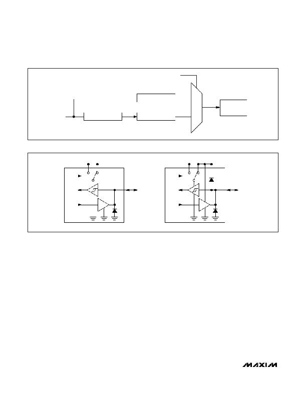
�SMBus/I� 2� C� Interfaced� 9-Port,�
�Level-Translating� GPIO� and� LED� Driver� with� CLA�
�PORT_� [5]�
�5-BIT� PWM�
�PORT_� [4:0]�
�0�
�I/O�
�CLOCK�
�3-BIT� PRESCALER�
�CONFIG26� [4:2]�
�4-BIT� BLINK�
�PORT_� [3:0]�
�1�
�Figure� 2.� Output� Port� Structure�
�SELECT�
�INPUT�
�OUTPUT�
�V+�
�P1�
�V� LA�
�PORT� P1�
�SELECT�
�INPUT�
�OUTPUT�
�V+�
�P2–P9�
�V� LA�
�PORT�
�P2–P9�
�Figure� 3.� Port� I/O� Structure�
�Ports� P2–P9� are� overvoltage� protected� to� V� LA� .� This� is� true�
�even� for� a� port� used� as� an� input� with� a� V� DD� port� logic-�
�input� threshold.� Port� P1� is� overvoltage� protected� to� 5.5V,�
�independent� of� V� DD� and� V� LA� (see� Figure� 3).� To� mix� logic�
�outputs� with� more� than� one� voltage� swing� on� a� group� of�
�ports� using� the� same� port� supply,� set� the� port� supply� volt-�
�age� (V� LA� )� to� be� the� highest� output� voltage.� Use� push-pull�
�outputs� and� port� P1� for� the� highest� voltage� ports,� and� use�
�open-drain� outputs� with� external� pullup� resistors� for� the�
�lower� voltage� ports.� When� P2–P9� are� acting� as� inputs� ref-�
�erenced� to� V� DD� ,� make� sure� the� V� LA� voltage� is� greater�
�than� V� DD� -� 0.3V.�
�Port� Lock� Registers�
�Use� the� port� lock� registers� to� lock� any� combination� of�
�port� I/O� register� functionality� (see� Table� 8).� The� port�
�lock� registers� are� unlocked� on� power-up� or� by� configur-�
�ing� the� RSTPOR� bit� to� reset� to� POR� value.� The� bits� in�
�the� port� lock� register� can� only� be� written� to� once.� After�
�setting� a� bit� to� logic-high,� the� bit� can� only� be� cleared�
�by� powering� off� the� device.�
�When� a� bit� position� in� the� port� lock� register� is� set,� the�
�corresponding� port� I/O� registers� cannot� change.� When� a�
�port� I/O� register� is� locked� as� an� output,� none� of� its� output�
�register� settings� can� change.� When� a� port� I/O� register� is�
�locked� as� an� input,� only� bits� D0� and� D1� can� change,� and�
�the� locked� input� behaviour� options,� such� as� debounce�
�and� transition� detection,� operate� as� normal.�
�Input� Debounce�
�The� MAX7302� samples� the� input� ports� every� 31ms� if�
�input� debouncing� is� enabled� for� an� input� port� (D2� =� 1�
�of� the� port� I/O� register).� The� MAX7302� compares� each�
�new� sample� with� the� previous� sample.� If� the� new� sam-�
�ple� and� the� previous� sample� have� the� same� value,� the�
�corresponding� internal� register� updates.�
�When� the� port� input� is� read� through� the� serial� interface,�
�the� MAX7302� does� not� return� the� instantaneous� value�
�of� the� logic� level� from� the� port� because� debounce� is�
�active.� Instead,� the� MAX7302� returns� the� stored�
�debounced� input� signal.�
�12�
�______________________________________________________________________________________�
�相关PDF资料 |
PDF描述 |
|---|---|
| NCP612SQ25T1G | IC REG LDO 2.5V .2A SOT-353 |
| VE-J3L-CX-F2 | CONVERTER MOD DC/DC 28V 75W |
| B82442A1474K | INDUCTOR 470UH 120MA 2220 10% |
| VE-J3L-CX-F1 | CONVERTER MOD DC/DC 28V 75W |
| AISC-0402-47NJ-T | INDUCTOR WW CERAM 47.0NH 0402 |
相关代理商/技术参数 |
参数描述 |
|---|---|
| MAX7302ATE | 制造商:MAXIM 制造商全称:Maxim Integrated Products 功能描述:SMBus/I2C Interfaced 9-Port, Level-Translating GPIO and LED Driver with CLA |
| MAX7302ATE/GH9 | 制造商:Maxim Integrated Products 功能描述:LEVEL-TRANSLATING GPIO AND LED DRIVER WITH CLA - Rail/Tube |
| MAX7302ATE+ | 功能描述:外围驱动器与原件 - PCI 9-Port Level-Trans GPIO & LED Driver RoHS:否 制造商:PLX Technology 工作电源电压: 最大工作温度: 安装风格:SMD/SMT 封装 / 箱体:FCBGA-1156 封装:Tray |
| MAX7302ATE+T | 功能描述:外围驱动器与原件 - PCI 9-Port Level-Trans GPIO & LED Driver RoHS:否 制造商:PLX Technology 工作电源电压: 最大工作温度: 安装风格:SMD/SMT 封装 / 箱体:FCBGA-1156 封装:Tray |
| MAX7302EVKIT+ | 制造商:Maxim Integrated Products 功能描述:MAX7302 EVAL KIT - Boxed Product (Development Kits) |
发布紧急采购,3分钟左右您将得到回复。