- 您现在的位置:买卖IC网 > PDF目录20966 > MAX7306AUB+ (Maxim Integrated)IC LED DRIVER LINEAR 10-UMAX PDF资料下载
参数资料
| 型号: | MAX7306AUB+ |
| 厂商: | Maxim Integrated |
| 文件页数: | 14/23页 |
| 文件大小: | 0K |
| 描述: | IC LED DRIVER LINEAR 10-UMAX |
| 产品培训模块: | Lead (SnPb) Finish for COTS Obsolescence Mitigation Program |
| 标准包装: | 50 |
| 拓扑: | PWM |
| 输出数: | 4 |
| 内部驱动器: | 是 |
| 类型 - 主要: | 背光,LED 闪烁器 |
| 类型 - 次要: | 白色 LED |
| 频率: | 1MHz |
| 电源电压: | 1.62 V ~ 3.6 V |
| 安装类型: | 表面贴装 |
| 封装/外壳: | 10-TFSOP,10-MSOP(0.118",3.00mm 宽)裸露焊盘 |
| 供应商设备封装: | 10-µMAX-EP |
| 包装: | 管件 |
| 工作温度: | -40°C ~ 125°C |
�� �
�
�SMBus/I� 2� C� Interfaced� 4-Port,� Level-Translating�
�GPIOs� and� LED� Drivers�
�the� host� processor� of� data� changes� at� the� selected�
�inputs.� Reset� INT� by� reading� any� port’s� I/O� registers�
�(0x01� to� 0x04).�
�Standby� Mode�
�Upon� power-up,� the� MAX7306/MAX7307� enter� standby�
�mode� when� the� serial� interface� is� idle.� If� any� of� the� PWM�
�intensity� control,� blink,� or� debounce� features� are� used,�
�the� operating� current� rises� because� the� internal� PWM�
�oscillator� is� running� and� toggling� counters.� When� using�
�OSCIN� to� override� the� internal� oscillator,� the� operating�
�current� varies� according� to� the� frequency� at� OSCIN.�
�When� the� serial� interface� is� active,� the� operating� current�
�also� increases� because� the� MAX7306/MAX7307,� like� all�
�I� 2� C� slaves,� have� to� monitor� every� transmission.� The� bus�
�timeout� circuit� and� debounce� circuit� use� the� internal� oscil-�
�lator� even� if� OSCIN� is� selected.�
�Internal� Oscillator� and� OSCIN/OSCOUT�
�External� Clock� Options�
�The� MAX7306/MAX7307� contain� an� internal� oscillator�
�nominally� at� 32kHz.� The� MAX7306/MAX7307� always� use�
�the� internal� oscillator� for� bus� timeout� and� for� debounce�
�timing� (when� enabled).� The� internal� oscillator� is� also�
�used� by� default� to� generate� PWM� and� blink� timing.� The�
�internal� oscillator� only� runs� when� the� clock� output�
�OSCOUT� is� needed� to� keep� the� operating� current� as�
�low� as� possible.�
�The� MAX7306/MAX7307� can� use� an� external� clock�
�source� instead� of� the� internal� oscillator� for� the� PWM�
�and� blink� timing.� The� external� clock� can� range� from� DC�
�to� 1MHz� and� it� connects� to� the� P2/OSCIN� port.� The�
�P3/OSCOUT� port� provides� a� buffered� and� level-shifted�
�output� of� the� internal� oscillator� or� external� clock� to� drive�
�other� devices.� Select� the� P2/OSCIN� and� P3/OSCOUT�
�port� options� using� the� device� configuration� register�
�0x27� bits� D2� and� D3� (see� Table� 2).�
�The� P2/OSCIN� port� is� overvoltage� protected� to� supply�
�voltage� V� LA� for� the� MAX7307,� so� the� external� clock� can�
�exceed� V� DD� if� V� LA� is� greater� than� V� DD� .� The� external�
�clock� cannot� exceed� V� DD� for� the� MAX7306.� The� port� P2�
�register� (see� Tables� 2� and� 6)� sets� the� P2/OSCIN� logic�
�threshold� (30%/70%)� to� either� the� V� DD� supply� or� the� V� LA� .�
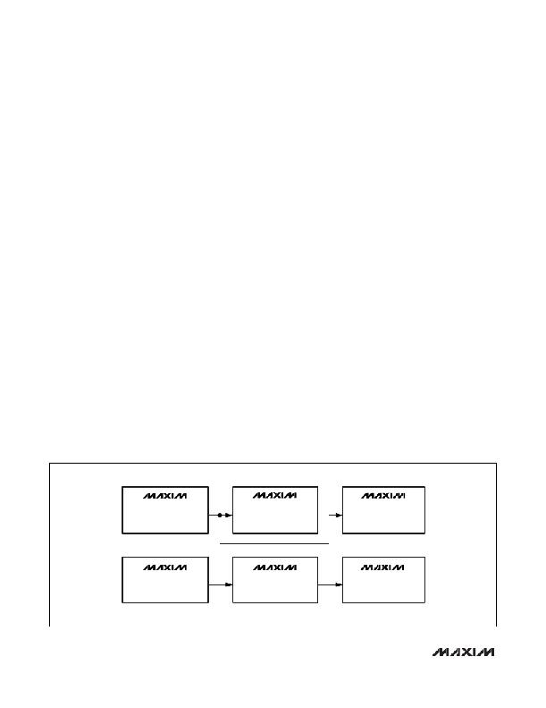
�Use� OSCOUT� or� an� external� clock� source� to� cascade�
�up� to� four� MAX7306s� per� master� for� applications� requir-�
�ing� additional� ports.� To� synchronize� the� blink� action�
�across� multiple� MAX7306s� (see� Figures� 4� and� 5),� use�
�OSCOUT� from� one� MAX7306� to� drive� OSCIN� of� the�
�other� MAX7306s.� This� process� ensures� the� same� blink�
�frequency� of� all� the� devices,� but� also� make� sure� to� syn-�
�chronize� the� blink� phase.� The� blink� timing� of� multiple�
�MAX7306s� is� synchronous� at� the� instant� of� power-up�
�because� the� blink� and� PWM� counters� clear� by� each�
�device� ’s� internal� reset� circuit,� and� by� default� the�
�device’s� internal� oscillators� are� off� upon� power-up.�
�Ensure� that� the� blink� phase� of� all� the� devices� remains�
�synchronized� by� programming� the� OSCIN� and�
�OSCOUT� functionality� before� programming� any� feature�
�that� causes� a� MAX7306’s� internal� oscillator� to� operate�
�(blink,� PWM,� bus� timeout,� or� key� debounce).� Configure�
�the� RST� input� to� reset� the� internal� timing� counters� used�
�for� PWM� and� blink� by� setting� bit� D1� of� device� configu-�
�ration� register� 0x26� (see� Table� 3).�
�MAX7306/MAX7307�
�P3/OSCOUT�
�MAX7306/MAX7307�
�MAX7306/MAX7307�
�P2/OSCIN�
�MAX7306/MAX7307�
�MAX7306/MAX7307�
�P2/OSCIN�
�MAX7306/MAX7307�
�P3/OSCOUT�
�P2/OSCIN�
�P3/OSCOUT�
�P2/OSCIN�
�Figure� 4.� Synchronizing� Multiple� MAX7306/MAX7307s� (Internal� Oscillator)�
�14�
�______________________________________________________________________________________�
�相关PDF资料 |
PDF描述 |
|---|---|
| REC3-243.3SRWZ/H2/A/M/SMD-R | CONV DC/DC 3W 9-36VIN 3.3VOUT |
| REC8-1215SRW/H2/A/M/SMD-R | CONV DC/DC 8W 12VIN 15VOUT |
| REC3-053.3SRW/H2/A/M/SMD/CTRL-R | CONV DC/DC 3W 4.5-9VIN 3.3VOUT |
| P51-1000-S-C-P-4.5V-000-000 | SENSOR 1000PSI M12-1.5 6G 4.5V |
| P51-200-A-O-MD-20MA-000-000 | SENSOR 200PSI 7/16-20UNF 2B 20MA |
相关代理商/技术参数 |
参数描述 |
|---|---|
| MAX7306AUB+ | 功能描述:外围驱动器与原件 - PCI 4-Port Level-Trans GPIO & LED Driver RoHS:否 制造商:PLX Technology 工作电源电压: 最大工作温度: 安装风格:SMD/SMT 封装 / 箱体:FCBGA-1156 封装:Tray |
| MAX7306AUB+T | 功能描述:外围驱动器与原件 - PCI 4-Port Level-Trans GPIO & LED Driver RoHS:否 制造商:PLX Technology 工作电源电压: 最大工作温度: 安装风格:SMD/SMT 封装 / 箱体:FCBGA-1156 封装:Tray |
| MAX7306EVKIT+ | 制造商:Maxim Integrated Products 功能描述:MAX7306 EVAL KIT/EVAL SYS - Rail/Tube |
| MAX7307 | 制造商:MAXIM 制造商全称:Maxim Integrated Products 功能描述:SMBus/I2C Interfaced 4-Port, Level-Translating GPIOs and LED Drivers |
| MAX7307ALB+ | 制造商:Maxim Integrated Products 功能描述:- Rail/Tube |
发布紧急采购,3分钟左右您将得到回复。