- 您现在的位置:买卖IC网 > PDF目录3774 > MAX7322AEE+ (Maxim Integrated Products)IC I/O EXPANDER I2C 4B 16QSOP PDF资料下载
参数资料
| 型号: | MAX7322AEE+ |
| 厂商: | Maxim Integrated Products |
| 文件页数: | 17/18页 |
| 文件大小: | 0K |
| 描述: | IC I/O EXPANDER I2C 4B 16QSOP |
| 产品培训模块: | Lead (SnPb) Finish for COTS Obsolescence Mitigation Program |
| 标准包装: | 100 |
| 接口: | I²C |
| 输入/输出数: | 4 |
| 中断输出: | 是 |
| 频率 - 时钟: | 400kHz |
| 电源电压: | 1.7 V ~ 5.5 V |
| 工作温度: | -40°C ~ 125°C |
| 安装类型: | 表面贴装 |
| 封装/外壳: | 16-SSOP(0.154",3.90mm 宽) |
| 供应商设备封装: | 16-QSOP |
| 包装: | 管件 |
| 包括: | POR |
MAX7322
I2C Port Expander with
4 Push-Pull Outputs and 4 Inputs
8
_______________________________________________________________________________________
PIN
CONNECTION
DEVICE ADDRESS
OUTPUTS POWER—UP DEFAULT
40k
Ω INPUT PULLUPS
ENABLED
AD2
AD0
A6
A5A4A3
A2A1A0
O7
O6
I5
I4
I3
I2
O1
O0
O7 O6
I5
I4
I3
I2
O1 O0
SCL
GND
1
100
000
1
0
Y
— —
SCL
V+
1
100
001
1
Y
SCL
1
0
1
0
1
Y
SCL
SDA
1
0
1
Y
SDA
GND
1
100
1
0
Y
— —
SDA
V+
1
100
101
1
Y
SDA
SCL
1
0
1
0
1
Y
SDA
1
0
1
Y
GND
1
101
000
0
—
— — —
GND
V+
1
101
001
0
1
—
Y
GND
SCL
1
101
010
0
1
—
Y
GND
SDA
1
101
011
0
1
—
Y
V+
GND
1
101
100
1
0
Y
— —
V+
1
101
1
Y
V+
SCL
1
101
110
1
Y
V+
SDA
1
101
111
1
Inputs
11
Pullups
are
not
enabled
for
push-pull
outputs
YY
Y
Pullups
are
not
enabled
for
push-pull
outputs
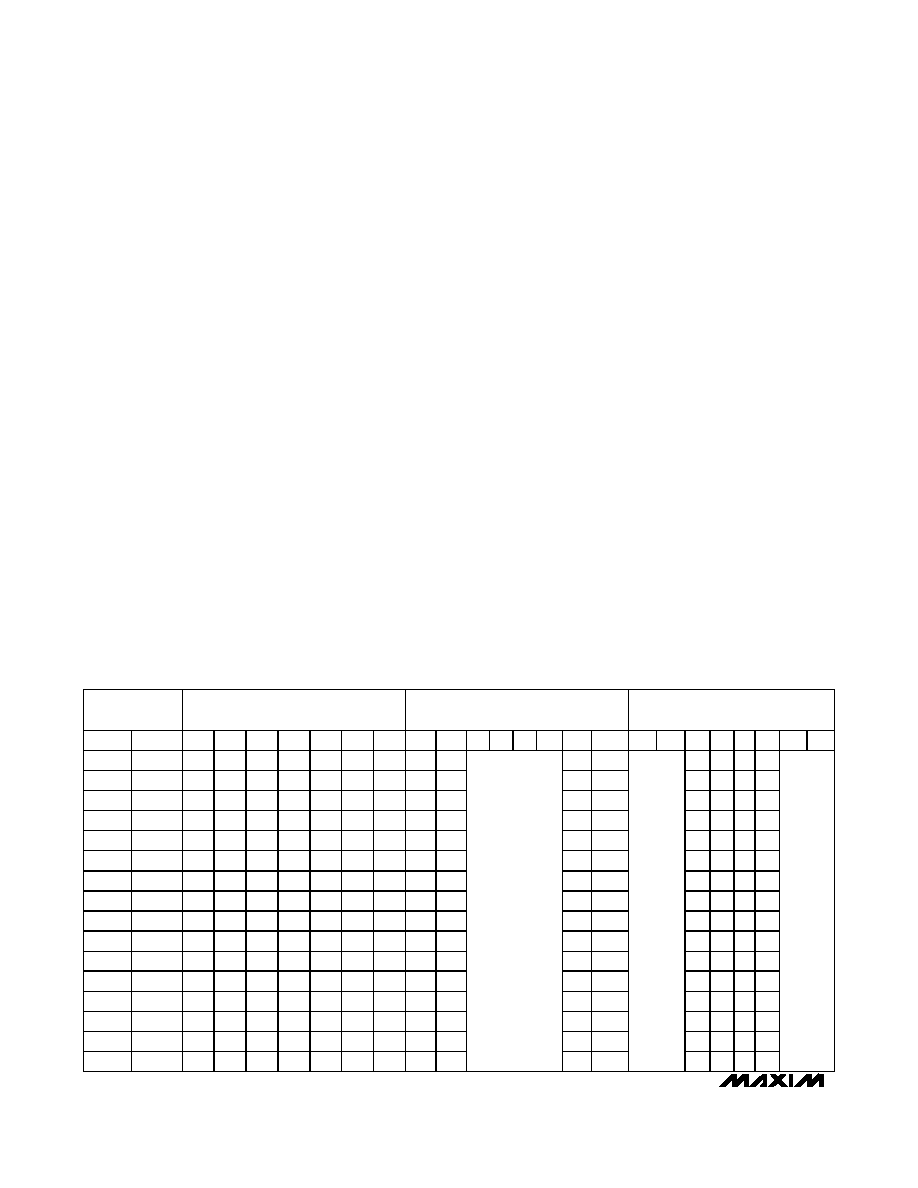
Table 2. MAX7322 Address Map
On initial power-up, the MAX7322 cannot decode the
address inputs AD2 and AD0 fully until the first I2C
transmission. AD0 and AD2 initially appear to be con-
nected to V+ or GND. This is important because the
address selection determines the power-up logic state,
and whether pullups are enabled. However, at power-
up, the I2C SDA and SCL bus interface lines are high
impedance at the pins of every device (master or slave)
connected to the bus, including the MAX7322. This is
guaranteed as part of the I2C specification. Therefore,
address inputs AD2 and AD0 that are connected to
SDA or SCL normally appear at power-up to be connect-
ed to V+. The port selection logic uses AD0 to select
whether pullups are enabled for ports I2 and I3, and to
set the initial logic state for ports O0 and O1. AD2
selects whether pullups are enabled for ports I4 and I5
and sets the internal logic state for ports O6 and O7. The
rule is that a logic-high, SDA, or SCL connection selects
the pullups and sets the default logic state high. A logic-
low deselects the pullups and sets the default logic state
low (Table 2). This means that the port configuration is
correct on power-up for a standard I2C configuration,
where SDA or SCL are pulled up to V+ by the external I2C
pullup resistors.
There are circumstances where the assumption that
SDA = SCL = V+ on power-up is not true—for example,
in applications in which there is legitimate bus activity
during power-up. Also, if SDA and SCL are terminated
with pullup resistors to a different supply voltage than
the MAX7322’s supply voltage, and if that pullup supply
rises later than the MAX7322’s supply, then SDA or
SCL may appear at power-up to be connected to GND.
In such applications, use the four address combina-
tions that are selected by connecting address inputs
AD2 and AD0 to V+ or GND (shown in bold in Table 2).
These selections are guaranteed to be correct at
power-up, independent of SDA and SCL behavior. If
one of the other 12 address combinations is used, an
unexpected combination of pullups might be asserted
until the first I2C transmission (to any device, not neces-
sarily the MAX7322) is put on the bus, and an unexpect-
ed combination of ports may initialize as logic-low
outputs instead of inputs or logic-high outputs.
Port Inputs
Port inputs switch at CMOS logic levels as determined by
the expander’s supply voltage, and are overvoltage toler-
ant to +6V, independent of the expander’s supply voltage.
Port Input Transition Detection
All four input ports are monitored for changes since the
expander was last accessed through the serial inter-
face. The state of the I/O ports is stored in an internal
相关PDF资料 |
PDF描述 |
|---|---|
| MAX7310AUE+ | IC I/O EXPANDER I2C 8B 16TSSOP |
| MAX7317ATE+ | IC I/O EXPANDER SPI 10B 16TQFN |
| MAX7317AEE+ | IC I/O EXPANDER SPI 10B 16QSOP |
| MAX7315ATE+ | IC I/O EXPANDER I2C 8B 16TQFN-EP |
| MAX7321ATE+ | IC I/O EXPANDER I2C 8B 16TQFN-EP |
相关代理商/技术参数 |
参数描述 |
|---|---|
| MAX7322AEE+ | 功能描述:接口-I/O扩展器 I2C Port Expander w/4 P-P Out & 4 In RoHS:否 制造商:NXP Semiconductors 逻辑系列: 输入/输出端数量: 最大工作频率:100 kHz 工作电源电压:1.65 V to 5.5 V 工作温度范围:- 40 C to + 85 C 安装风格:SMD/SMT 封装 / 箱体:HVQFN-16 封装:Reel |
| MAX7322AEE+T | 功能描述:接口-I/O扩展器 I2C Port Expander w/4 P-P Out & 4 In RoHS:否 制造商:NXP Semiconductors 逻辑系列: 输入/输出端数量: 最大工作频率:100 kHz 工作电源电压:1.65 V to 5.5 V 工作温度范围:- 40 C to + 85 C 安装风格:SMD/SMT 封装 / 箱体:HVQFN-16 封装:Reel |
| MAX7322AEE-T | 功能描述:接口-I/O扩展器 RoHS:否 制造商:NXP Semiconductors 逻辑系列: 输入/输出端数量: 最大工作频率:100 kHz 工作电源电压:1.65 V to 5.5 V 工作温度范围:- 40 C to + 85 C 安装风格:SMD/SMT 封装 / 箱体:HVQFN-16 封装:Reel |
| MAX7322ATE | 功能描述:接口-I/O扩展器 I2C Port Expander w/4 P-P Out & 4 In RoHS:否 制造商:NXP Semiconductors 逻辑系列: 输入/输出端数量: 最大工作频率:100 kHz 工作电源电压:1.65 V to 5.5 V 工作温度范围:- 40 C to + 85 C 安装风格:SMD/SMT 封装 / 箱体:HVQFN-16 封装:Reel |
| MAX7322ATE+ | 功能描述:接口-I/O扩展器 I2C Port Expander w/4 P-P Out & 4 In RoHS:否 制造商:NXP Semiconductors 逻辑系列: 输入/输出端数量: 最大工作频率:100 kHz 工作电源电压:1.65 V to 5.5 V 工作温度范围:- 40 C to + 85 C 安装风格:SMD/SMT 封装 / 箱体:HVQFN-16 封装:Reel |
发布紧急采购,3分钟左右您将得到回复。