- 您现在的位置:买卖IC网 > PDF目录3774 > MAX7322AEE+ (Maxim Integrated Products)IC I/O EXPANDER I2C 4B 16QSOP PDF资料下载
参数资料
| 型号: | MAX7322AEE+ |
| 厂商: | Maxim Integrated Products |
| 文件页数: | 2/18页 |
| 文件大小: | 0K |
| 描述: | IC I/O EXPANDER I2C 4B 16QSOP |
| 产品培训模块: | Lead (SnPb) Finish for COTS Obsolescence Mitigation Program |
| 标准包装: | 100 |
| 接口: | I²C |
| 输入/输出数: | 4 |
| 中断输出: | 是 |
| 频率 - 时钟: | 400kHz |
| 电源电压: | 1.7 V ~ 5.5 V |
| 工作温度: | -40°C ~ 125°C |
| 安装类型: | 表面贴装 |
| 封装/外壳: | 16-SSOP(0.154",3.90mm 宽) |
| 供应商设备封装: | 16-QSOP |
| 包装: | 管件 |
| 包括: | POR |
SDA operates as both an input and an open-drain out-
put. A pullup resistor, typically 4.7k
Ω, is required on
SDA. SCL operates only as an input. A pullup resistor,
typically 4.7k
Ω, is required on SCL if there are multiple
masters on the 2-wire interface, or if the master in a sin-
gle-master system has an open-drain SCL output.
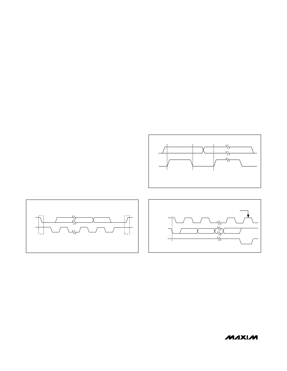
Each transmission consists of a START condition sent
by a master, followed by the MAX7322’s 7-bit slave
address plus R/W bit, one or more data bytes, and
finally a STOP condition (Figure 2).
START and STOP Conditions
Both SCL and SDA remain high when the interface is
not busy. A master signals the beginning of a transmis-
sion with a START (S) condition by transitioning SDA
from high to low while SCL is high. When the master
has finished communicating with the slave, the master
issues a STOP (P) condition by transitioning SDA from
low to high while SCL is high. The bus is then free for
another transmission (Figure 2).
Bit Transfer
One data bit is transferred during each clock pulse.
The data on SDA must remain stable while SCL is high
(Figure 3).
Acknowledge
The acknowledge bit is a clocked 9th bit the recipient
uses to acknowledge receipt of each byte of data
(Figure 4). Each byte transferred effectively requires 9
bits. The master generates the 9th clock pulse, and the
recipient pulls down SDA during the acknowledge
clock pulse, such that the SDA line is stable low during
the high period of the clock pulse. When the master is
transmitting to the MAX7322, the MAX7322 generates
the acknowledge bit because the device is the recipi-
ent. When the MAX7322 is transmitting to the master,
the master generates the acknowledge bit because the
master is the recipient.
MAX7322
I2C Port Expander with
4 Push-Pull Outputs and 4 Inputs
10
______________________________________________________________________________________
SDA
SCL
DATA LINE STABLE;
DATA VALID
CHANGE OF DATA
ALLOWED
Figure 3. Bit Transfer
SCL
SDA BY
TRANSMITTER
CLOCK PULSE
FOR ACKNOWLEDGMENT
START
CONDITION
SDA BY
RECEIVER
12
89
S
Figure 4. Acknowledge
SDA
SCL
START
CONDITION
STOP
CONDITION
SP
Figure 2. START and STOP Conditions
相关PDF资料 |
PDF描述 |
|---|---|
| MAX7310AUE+ | IC I/O EXPANDER I2C 8B 16TSSOP |
| MAX7317ATE+ | IC I/O EXPANDER SPI 10B 16TQFN |
| MAX7317AEE+ | IC I/O EXPANDER SPI 10B 16QSOP |
| MAX7315ATE+ | IC I/O EXPANDER I2C 8B 16TQFN-EP |
| MAX7321ATE+ | IC I/O EXPANDER I2C 8B 16TQFN-EP |
相关代理商/技术参数 |
参数描述 |
|---|---|
| MAX7322AEE+ | 功能描述:接口-I/O扩展器 I2C Port Expander w/4 P-P Out & 4 In RoHS:否 制造商:NXP Semiconductors 逻辑系列: 输入/输出端数量: 最大工作频率:100 kHz 工作电源电压:1.65 V to 5.5 V 工作温度范围:- 40 C to + 85 C 安装风格:SMD/SMT 封装 / 箱体:HVQFN-16 封装:Reel |
| MAX7322AEE+T | 功能描述:接口-I/O扩展器 I2C Port Expander w/4 P-P Out & 4 In RoHS:否 制造商:NXP Semiconductors 逻辑系列: 输入/输出端数量: 最大工作频率:100 kHz 工作电源电压:1.65 V to 5.5 V 工作温度范围:- 40 C to + 85 C 安装风格:SMD/SMT 封装 / 箱体:HVQFN-16 封装:Reel |
| MAX7322AEE-T | 功能描述:接口-I/O扩展器 RoHS:否 制造商:NXP Semiconductors 逻辑系列: 输入/输出端数量: 最大工作频率:100 kHz 工作电源电压:1.65 V to 5.5 V 工作温度范围:- 40 C to + 85 C 安装风格:SMD/SMT 封装 / 箱体:HVQFN-16 封装:Reel |
| MAX7322ATE | 功能描述:接口-I/O扩展器 I2C Port Expander w/4 P-P Out & 4 In RoHS:否 制造商:NXP Semiconductors 逻辑系列: 输入/输出端数量: 最大工作频率:100 kHz 工作电源电压:1.65 V to 5.5 V 工作温度范围:- 40 C to + 85 C 安装风格:SMD/SMT 封装 / 箱体:HVQFN-16 封装:Reel |
| MAX7322ATE+ | 功能描述:接口-I/O扩展器 I2C Port Expander w/4 P-P Out & 4 In RoHS:否 制造商:NXP Semiconductors 逻辑系列: 输入/输出端数量: 最大工作频率:100 kHz 工作电源电压:1.65 V to 5.5 V 工作温度范围:- 40 C to + 85 C 安装风格:SMD/SMT 封装 / 箱体:HVQFN-16 封装:Reel |
发布紧急采购,3分钟左右您将得到回复。