- 您现在的位置:买卖IC网 > PDF目录13330 > MAX795TESA+T (Maxim Integrated Products)IC SUPERVISOR MPU 8-SOIC PDF资料下载
参数资料
| 型号: | MAX795TESA+T |
| 厂商: | Maxim Integrated Products |
| 文件页数: | 16/20页 |
| 文件大小: | 0K |
| 描述: | IC SUPERVISOR MPU 8-SOIC |
| 产品培训模块: | Lead (SnPb) Finish for COTS Obsolescence Mitigation Program |
| 标准包装: | 2,500 |
| 类型: | 备用电池电路 |
| 监视电压数目: | 1 |
| 输出: | 开路漏极或开路集电极 |
| 复位: | 低有效 |
| 复位超时: | 最小为 140 ms |
| 电压 - 阀值: | 3.075V |
| 工作温度: | -40°C ~ 85°C |
| 安装类型: | 表面贴装 |
| 封装/外壳: | 8-SOIC(0.154",3.90mm 宽) |
| 供应商设备封装: | 8-SOIC |
| 包装: | 带卷 (TR) |
�� �
�
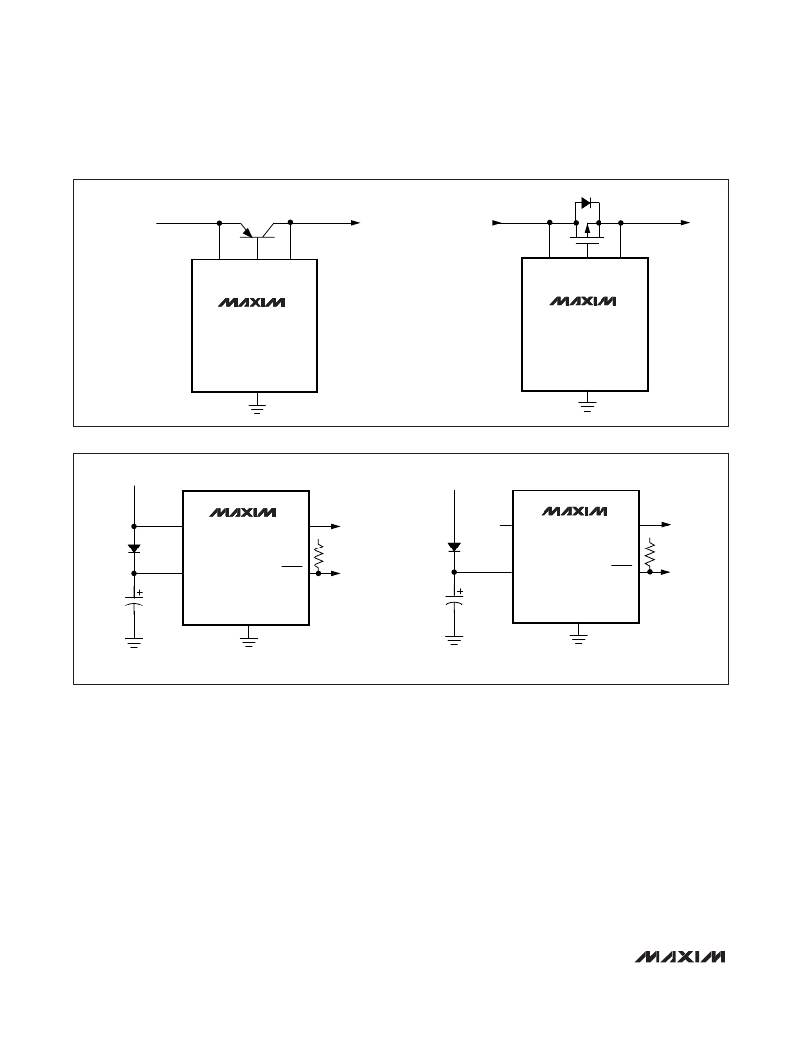
�3.0V/3.3V� Adjustable� Microprocessor�
�Supervisory� Circuits�
�PMOS� FET�
�BODY� DIODE�
�3.0V� OR� 3.3V�
�TO� CMOS� RAM�
�D�
�G�
�S�
�V� CC�
�BATT� ON�
�OUT�
�V� CC�
�BATT� ON�
�OUT�
�MAX793�
�MAX794�
�MAX795�
�GND�
�(a)�
�Figure� 14.� Driving� an� External� Transistor� with� BATT� ON�
�3.0V� OR� 3.3V�
�(b)�
�+5V�
�MAX793�
�MAX794�
�MAX795�
�GND�
�1N4148�
�V� CC�
�MAX793�
�MAX794�
�OUT�
�V� CC�
�TO� STATIC�
�RAM�
�3.0V� OR�
�3.3V�
�1N4148�
�V� CC�
�MAX793�
�MAX794�
�OUT�
�V� CC�
�TO� STATIC�
�RAM�
�BATT�
�RESET�
�TO� μ� P�
�BATT�
�RESET�
�TO� μ� P�
�(a)�
�0.47F�
�GND�
�(b)�
�0.47F�
�GND�
�Figure� 15.� Using� a� Super� Cap� as� a� Backup� Source�
�both� above� (V� H� )� and� below� (V� L� )� the� original� trip� point�
�Adding� Hysteresis� to� the� Power-Fail�
�Comparator� (MAX793/MAX794)�
�The� power-fail� comparator� has� a� typical� input� hystere-�
�sis� of� 10mV.� This� is� sufficient� for� most� applications�
�where� a� power-supply� line� is� being� monitored� through�
�an� external� voltage� divider� (see� the� section� Monitoring�
�an� Additional� Power� Supply).�
�If� additional� noise� margin� is� desired,� connect� a� resistor�
�between� PFO� and� PFI� as� shown� in� Figure� 16a.� Select�
�the� ratio� of� R1� and� R2� such� that� PFI� sees� V� PFT� when�
�V� IN� falls� to� its� trip� point� (V� TRIP� ).� R3� adds� the� additional�
�hysteresis� and� should� typically� be� more� than� 10� times�
�the� value� of� R1� or� R2.� The� hysteresis� window� extends�
�(V� TRIP� ).�
�Connecting� an� ordinary� signal� diode� in� series� with� R3,�
�as� shown� in� Figure� 16b,� causes� the� lower� trip� point� (V� L� )�
�to� coincide� with� the� trip� point� without� hysteresis� (V� TRIP� ),�
�so� the� entire� hysteresis� window� occurs� above� V� TRIP� .�
�This� method� provides� additional� noise� margin� without�
�compromising� the� accuracy� of� the� power-fail� threshold�
�when� the� monitored� voltage� is� falling.� It� is� useful� for�
�accurately� detecting� when� a� voltage� falls� past� a� thresh-�
�old.� The� current� through� R1� and� R2� should� be� at� least�
�1μA� to� ensure� that� the� 25nA� (max� over� temperature)�
�PFI� input� current� does� not� shift� the� trip� point.� R3� should�
�be� larger� than� 82k� ?� so� it� does� not� load� down� the� PFO�
�pin.� Capacitor� C1� is� optional,� and� adds� noise� rejection.�
�16�
�______________________________________________________________________________________�
�相关PDF资料 |
PDF描述 |
|---|---|
| RBA30DTBZ-S273 | CONN EDGECARD 60POS R/A .125 SLD |
| RGM18DTBH | CONN EDGECARD 36POS R/A .156 SLD |
| VE-25F-EY-F1 | CONVERTER MOD DC/DC 72V 50W |
| MAX705EUA+ | IC SUPERVISOR MPU 8-UMAX |
| HSC25DRYN-S13 | CONN EDGECARD 50POS .100 EXTEND |
相关代理商/技术参数 |
参数描述 |
|---|---|
| MAX796C/D | 功能描述:DC/DC 开关控制器 DICE SALES DICE RoHS:否 制造商:Texas Instruments 输入电压:6 V to 100 V 开关频率: 输出电压:1.215 V to 80 V 输出电流:3.5 A 输出端数量:1 最大工作温度:+ 125 C 安装风格: 封装 / 箱体:CPAK |
| MAX796CPE | 功能描述:DC/DC 开关控制器 RoHS:否 制造商:Texas Instruments 输入电压:6 V to 100 V 开关频率: 输出电压:1.215 V to 80 V 输出电流:3.5 A 输出端数量:1 最大工作温度:+ 125 C 安装风格: 封装 / 箱体:CPAK |
| MAX796CSE | 功能描述:DC/DC 开关控制器 RoHS:否 制造商:Texas Instruments 输入电压:6 V to 100 V 开关频率: 输出电压:1.215 V to 80 V 输出电流:3.5 A 输出端数量:1 最大工作温度:+ 125 C 安装风格: 封装 / 箱体:CPAK |
| MAX796CSE-T | 功能描述:DC/DC 开关控制器 RoHS:否 制造商:Texas Instruments 输入电压:6 V to 100 V 开关频率: 输出电压:1.215 V to 80 V 输出电流:3.5 A 输出端数量:1 最大工作温度:+ 125 C 安装风格: 封装 / 箱体:CPAK |
| MAX796EPE | 功能描述:DC/DC 开关控制器 RoHS:否 制造商:Texas Instruments 输入电压:6 V to 100 V 开关频率: 输出电压:1.215 V to 80 V 输出电流:3.5 A 输出端数量:1 最大工作温度:+ 125 C 安装风格: 封装 / 箱体:CPAK |
发布紧急采购,3分钟左右您将得到回复。