- 您现在的位置:买卖IC网 > PDF目录13556 > MAX857ESA+T (Maxim Integrated Products)IC REG BOOST ADJ 0.15A 8SOIC PDF资料下载
参数资料
| 型号: | MAX857ESA+T |
| 厂商: | Maxim Integrated Products |
| 文件页数: | 2/12页 |
| 文件大小: | 0K |
| 描述: | IC REG BOOST ADJ 0.15A 8SOIC |
| 产品培训模块: | Lead (SnPb) Finish for COTS Obsolescence Mitigation Program |
| 标准包装: | 2,500 |
| 类型: | 升压(升压) |
| 输出类型: | 可调式 |
| 输出数: | 1 |
| 输出电压: | 2.7 V ~ 6 V |
| 输入电压: | 0.8 V ~ 6 V |
| 频率 - 开关: | 500kHz |
| 电流 - 输出: | 150mA |
| 同步整流器: | 无 |
| 工作温度: | -40°C ~ 85°C |
| 安装类型: | 表面贴装 |
| 封装/外壳: | 8-SOIC(0.154",3.90mm 宽) |
| 包装: | 带卷 (TR) |
| 供应商设备封装: | 8-SOIC |
�� �
�
�3.3V/5V� or� Adjustable-Output,�
�Step-Up� DC-DC� Converters�
�ABSOLUTE� MAXIMUM� RATINGS�
�Supply� Voltage� (OUT� to� GND)� ...................................-0.3V,� +7V�
�Switch� Voltage� (LX� to� GND)� .......................................-0.3V,� +7V�
�—� —� —� –�
�S� H� D� N� ,� LBO� to� GND� ....................................................-0.3V,� +7V�
�–� –�
�LBI,� REF,� 3/� 5� ,� FB� to� GND� .........................-0.3V,� (V� OUT� +� 0.3V)�
�Reference� Current� (I� REF� )� ..................................................2.5mA�
�Continuous� Power� Dissipation� (T� A� =� +70°C)�
�SO� (derate� 5.88mW/°C� above� +70°C)� .........................471mW�
�μMAX� (derate� 4.1mW/°C� above� +70°C)� ......................330mW�
�Reverse� Battery� Current� (T� A� ≤� +45°C,� Note� 1)� .................750mA�
�Operating� Temperature� Ranges�
�MAX85_C_� _� ......................................................0°C� to� +70°C�
�MAX85_E_� _� ....................................................-40°C� to� +85°C�
�MAX85_MJA� .................................................-55°C� to� +125°C�
�Junction� Temperature� .....................................................+150°C�
�Storage� Temperature� Range� ............................-65°C� to� +160°C�
�Lead� Temperature� (soldering,� 10sec)� ............................+300°C�
�CERDIP� (derate� 8.00mW/°C� above� +70°C)� .................640mW�
�Note� 1:� Reverse� battery� current� is� measured� from� the� Typical� Operating� Circuit’s� battery� input� terminal� to� GND� when� the� battery� is�
�connected� backwards.� A� reverse� current� of� 750mA� will� not� exceed� the� SO� or� CERDIP� package� dissipation� limits� but,� if� left�
�for� an� extended� time� (more� than� ten� minutes),� may� degrade� performance.�
�Stresses� beyond� those� listed� under� “Absolute� Maximum� Ratings”� may� cause� permanent� damage� to� the� device.� These� are� stress� ratings� only,� and� functional�
�operation� of� the� device� at� these� or� any� other� conditions� beyond� those� indicated� in� the� operational� sections� of� the� specifications� is� not� implied.� Exposure� to�
�absolute� maximum� rating� conditions� for� extended� periods� may� affect� device� reliability.�
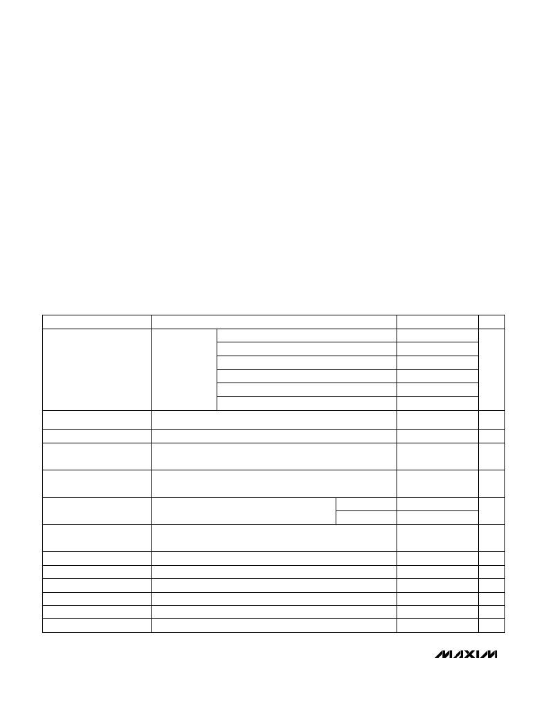
�ELECTRICAL� CHARACTERISTICS�
�(Circuits� of� Figure� 2,� V� IN� =� 2.5V,� I� LOAD� =� 0mA,� T� A� =� T� MIN� to� T� MAX� ,� unless� otherwise� noted.� Typical� values� are� at� T� A� =� +25°C.)�
�MAX856,� 3/� 5� =� 0V,� 0mA� ≤� I� LOAD� ≤� 100mA�
�MAX856,� 3/� 5� =� 3V,� 0mA� ≤� I� LOAD� ≤� 150mA�
�PARAMETER�
�CONDITIONS�
�–� –�
�–� –�
�MIN�
�4.80�
�3.17�
�TYP�
�5.0�
�3.3�
�MAX� UNITS�
�5.20�
�3.43�
�MAX858,� 3/� 5� =� 0V,� 0mA� ≤� I� LOAD� ≤� 25mA�
�Output� Voltage�
�2V� ≤� V� IN� ≤� 3V�
�MAX857,� V� OUT� =� 5V,� 0mA� ≤� I� LOAD� ≤� 100mA�
�–� –�
�4.80�
�4.80�
�5.0�
�5.0�
�5.20�
�5.20�
�V�
�MAX858,� 3/� 5� =� 3V,� 0mA� ≤� I� LOAD� ≤� 35mA�
�–� –�
�MAX859,� V� OUT� =� 5V,� 0mA� ≤� I� LOAD� ≤� 25mA�
�3.17�
�4.80�
�3.3�
�5.0�
�3.43�
�5.20�
�Minimum� Start-Up�
�Supply� Voltage�
�Minimum� Operating� Voltage�
�Quiescent� Supply� Current� in�
�3.3V� Mode� (Note� 2)�
�No� Load� Battery� Current�
�I� LOAD� =� 0mA�
�–� –�
�I� LOAD� =� 0mA,� 3/� 5� =� 3V,� LBI� =� 1.5V,� V� OUT� =� 3.47V,�
�(FB� =� 1.5V,� MAX857/MAX859� only)�
�Output� set� for� 3.3V,� measured� at� V� IN� in� Figure� 2,� R3� omitted.�
�0.8�
�0.8�
�25�
�60�
�1.8�
�60�
�V�
�V�
�μA�
�μA�
�Shutdown� Quiescent� Current�
�(Note� 2)�
�Peak� Inductor� Current� Limit�
�Reference� Voltage�
�–�
�—� —� —� –�
�S� H� D� N� =� 0V,� 3/� 5� =� 3V,� LBI� =� 1.5V,� V� OUT� =� 3.47V,�
�(FB� =� 1.5V,� MAX857/MAX859� only)�
�MAX856/MAX857�
�MAX858/MAX859�
�No� REF� load�
�MAX85_C�
�MAX85_E/M�
�1.23�
�1�
�500�
�125�
�1.25�
�1�
�5�
�1.27�
�μA�
�mA�
�V�
�Reference-Voltage� Regulation� 3/� 5� =� 3V,� -20μA� ≤� REF� load� ≤� 250μA,� C� REF� =� 0.22μF�
�–� –�
�0.8�
�2.0�
�%�
�LBI� Input� Threshold�
�With� falling� edge�
�1.22�
�1.25�
�1.28�
�V�
�LBI� Input� Hysteresis�
�25�
�mV�
�LBO� Output� Voltage� Low�
�LBO� Output� Leakage� Current�
�I� SINK� =� 2mA�
�LBO� =� 5V�
�0.4�
�1�
�V�
�μA�
�2�
�_______________________________________________________________________________________�
�相关PDF资料 |
PDF描述 |
|---|---|
| 25YXJ2200M12.5X25 | CAP ALUM 2200UF 25V 20% RADIAL |
| GCC26DRXH-S734 | CONN EDGECARD 52POS DIP .100 SLD |
| MAX6760TARGD3+T | IC DETECT VOLT WINDOW 8-TDFN |
| AVS335M35A12T-F | CAP ALUM 3.3UF 35V 20% SMD |
| VI-2TM-EX-F2 | CONVERTER MOD DC/DC 10V 75W |
相关代理商/技术参数 |
参数描述 |
|---|---|
| MAX8581ETB+T | 功能描述:直流/直流开关转换器 2.5/1.5MHz Step-Down Converter RoHS:否 制造商:STMicroelectronics 最大输入电压:4.5 V 开关频率:1.5 MHz 输出电压:4.6 V 输出电流:250 mA 输出端数量:2 最大工作温度:+ 85 C 安装风格:SMD/SMT |
| MAX8582ETB+ | 制造商:Maxim Integrated Products 功能描述: |
| MAX8582ETB+T | 功能描述:直流/直流开关转换器 2.5/1.5MHz Step-Down Converter RoHS:否 制造商:STMicroelectronics 最大输入电压:4.5 V 开关频率:1.5 MHz 输出电压:4.6 V 输出电流:250 mA 输出端数量:2 最大工作温度:+ 85 C 安装风格:SMD/SMT |
| MAX8582EVKIT+ | 制造商:Maxim Integrated Products 功能描述:MAX8582 EVAL KIT - Rail/Tube |
| MAX8585EUA | 功能描述:功率驱动器IC RoHS:否 制造商:Micrel 产品:MOSFET Gate Drivers 类型:Low Cost High or Low Side MOSFET Driver 上升时间: 下降时间: 电源电压-最大:30 V 电源电压-最小:2.75 V 电源电流: 最大功率耗散: 最大工作温度:+ 85 C 安装风格:SMD/SMT 封装 / 箱体:SOIC-8 封装:Tube |
发布紧急采购,3分钟左右您将得到回复。