- 您现在的位置:买卖IC网 > PDF目录13556 > MAX857ESA+T (Maxim Integrated Products)IC REG BOOST ADJ 0.15A 8SOIC PDF资料下载
参数资料
| 型号: | MAX857ESA+T |
| 厂商: | Maxim Integrated Products |
| 文件页数: | 6/12页 |
| 文件大小: | 0K |
| 描述: | IC REG BOOST ADJ 0.15A 8SOIC |
| 产品培训模块: | Lead (SnPb) Finish for COTS Obsolescence Mitigation Program |
| 标准包装: | 2,500 |
| 类型: | 升压(升压) |
| 输出类型: | 可调式 |
| 输出数: | 1 |
| 输出电压: | 2.7 V ~ 6 V |
| 输入电压: | 0.8 V ~ 6 V |
| 频率 - 开关: | 500kHz |
| 电流 - 输出: | 150mA |
| 同步整流器: | 无 |
| 工作温度: | -40°C ~ 85°C |
| 安装类型: | 表面贴装 |
| 封装/外壳: | 8-SOIC(0.154",3.90mm 宽) |
| 包装: | 带卷 (TR) |
| 供应商设备封装: | 8-SOIC |
�� �
�
�3.3V/5V� or� Adjustable-Output,�
�Step-Up� DC-DC� Converters�
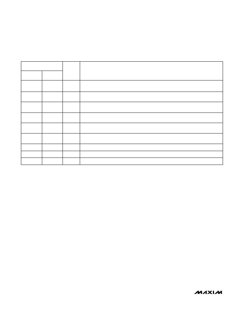
�______________________________________________________________Pin� Description�
�PIN�
�MAX856�
�MAX858�
�1�
�2�
�—�
�3�
�4�
�5�
�6�
�7�
�8�
�MAX857�
�MAX859�
�1�
�—�
�2�
�3�
�4�
�5�
�6�
�7�
�8�
�NAME�
�–� —� —� —� –�
�S� H� D� N�
�–� –�
�3/� 5�
�FB�
�REF�
�LBO�
�LBI�
�OUT�
�GND�
�LX�
�FUNCTION�
�Shutdown� Input.� When� low,� the� entire� circuit� is� off� and� V� OUT� =� V� IN� -� V� D,� where� V� D� is� the�
�forward� voltage� drop� of� the� external� Schottky� rectifier.�
�Selects� the� output� voltage;� connect� to� GND� for� 5V� output,� and� to� OUT� for� 3.3V�
�output.�
�Feedback� Input� for� adjustable-output� operation.� Connect� to� an� external� resistor� voltage�
�divider� between� OUT� and� GND.�
�1.25V� Reference� Voltage� Output.� Bypass� with� 0.22μF� to� GND� (0.1μF� if� there� is� no� external�
�reference� load).� Maximum� load� capability� is� 250μA� source,� 20μA� sink.�
�Low-Battery� Output.� An� open-drain� N-channel� MOSFET� sinks� current� when� the� voltage� at�
�LBI� drops� below� 1.25V.�
�Low-Battery� Input.� When� the� voltage� on� LBI� drops� below� 1.25V,� LBO� sinks� current.�
�If� not� used,� connect� to� V� IN� .�
�Connect� OUT� to� the� regulator� output.� OUT� provides� bootstrap� power� to� the� IC.�
�Power� Ground.� Must� be� low� impedance;� solder� directly� to� ground� plane.�
�N-Channel� Power-MOSFET� Drain�
�_______________Detailed� Description�
�Operating� Principle�
�The� MAX856–MAX859� combine� a� switch-mode� regula-�
�tor,� N-channel� power� MOSFET,� precision� voltage� refer-�
�ence,� and� power-fail� detector� in� a� single� monolithic�
�device.� The� MOSFET� is� a� “sense-FET”� type� for� best�
�efficiency,� and� has� a� very� low� gate� threshold� voltage� to�
�ensure� start-up� with� low� battery� voltages� (0.8V� typ).�
�PFM� Control� Scheme�
�A� unique� minimum-off-time,� current-limited� pulse-fre-�
�quency� modulation� (PFM)� control� scheme� is� a� key� fea-�
�ture� of� the� MAX856� series� (Figure� 1).� This� scheme�
�combines� the� high� output� power� and� efficiency� of� a�
�pulse-width� modulation� (PWM)� device� with� the� ultra-low�
�quiescent� current� of� a� traditional� PFM� pulse-skipper.�
�There� is� no� oscillator;� at� heavy� loads,� switching� is�
�accomplished� through� a� constant-peak-current� limit� in�
�the� switch,� which� allows� the� inductor� current� to� vary�
�between� this� peak� limit� and� some� lesser� value.� At� light�
�loads,� switching� frequency� is� governed� by� a� pair� of�
�one-shots,� which� set� a� minimum� off-time� (1μs)� and� a�
�maximum� on-time� (4μs).� The� switching� frequency�
�depends� upon� the� load� and� the� input� voltage,� and� can�
�range� up� to� 500kHz.�
�The� peak� switch� current� of� the� internal� MOSFET� power�
�switch� is� fixed� at� 500mA� ±100mA� (MAX856/MAX857)�
�or� 125mA� ±25mA� (MAX858/MAX859).� The� switch’s� on-�
�resistance� is� typically� 1� ?� (MAX856/MAX857)� or� 4� ?�
�(MAX858/MAX859),� resulting� in� a� switch� voltage� drop�
�(V� SW� )� of� about� 500mV� under� high� output� loads.� The�
�value� of� V� SW� will� decrease� with� light� current� loads.�
�Conventional� PWM� converters� generate� constant-fre-�
�quency� switching� noise,� whereas� the� unique� architec-�
�ture� of� the� MAX856–MAX859� produces� variable-fre-�
�quency� switching� noise.� However,� unlike� conventional�
�pulse-skippers� (where� noise� amplitude� varies� with� input�
�voltage),� noise� in� the� MAX856� series� does� not� exceed�
�the� switch� current� limit� times� the� filter-capacitor� equiva-�
�lent� series� resistance� (ESR).�
�Voltage� Reference�
�The� precision� voltage� reference� is� suitable� for� driving�
�external� loads,� such� as� an� analog-to-digital� converter.�
�The� voltage-reference� output� changes� less� than� ±2%�
�when� sourcing� up� to� 250μA� and� sinking� up� to� 20μA.� If�
�the� reference� drives� an� external� load,� bypass� it� with�
�0.22μF� to� GND.� If� the� reference� is� unloaded,� bypass� it�
�with� at� least� 0.1μF.�
�6�
�_______________________________________________________________________________________�
�相关PDF资料 |
PDF描述 |
|---|---|
| 25YXJ2200M12.5X25 | CAP ALUM 2200UF 25V 20% RADIAL |
| GCC26DRXH-S734 | CONN EDGECARD 52POS DIP .100 SLD |
| MAX6760TARGD3+T | IC DETECT VOLT WINDOW 8-TDFN |
| AVS335M35A12T-F | CAP ALUM 3.3UF 35V 20% SMD |
| VI-2TM-EX-F2 | CONVERTER MOD DC/DC 10V 75W |
相关代理商/技术参数 |
参数描述 |
|---|---|
| MAX8581ETB+T | 功能描述:直流/直流开关转换器 2.5/1.5MHz Step-Down Converter RoHS:否 制造商:STMicroelectronics 最大输入电压:4.5 V 开关频率:1.5 MHz 输出电压:4.6 V 输出电流:250 mA 输出端数量:2 最大工作温度:+ 85 C 安装风格:SMD/SMT |
| MAX8582ETB+ | 制造商:Maxim Integrated Products 功能描述: |
| MAX8582ETB+T | 功能描述:直流/直流开关转换器 2.5/1.5MHz Step-Down Converter RoHS:否 制造商:STMicroelectronics 最大输入电压:4.5 V 开关频率:1.5 MHz 输出电压:4.6 V 输出电流:250 mA 输出端数量:2 最大工作温度:+ 85 C 安装风格:SMD/SMT |
| MAX8582EVKIT+ | 制造商:Maxim Integrated Products 功能描述:MAX8582 EVAL KIT - Rail/Tube |
| MAX8585EUA | 功能描述:功率驱动器IC RoHS:否 制造商:Micrel 产品:MOSFET Gate Drivers 类型:Low Cost High or Low Side MOSFET Driver 上升时间: 下降时间: 电源电压-最大:30 V 电源电压-最小:2.75 V 电源电流: 最大功率耗散: 最大工作温度:+ 85 C 安装风格:SMD/SMT 封装 / 箱体:SOIC-8 封装:Tube |
发布紧急采购,3分钟左右您将得到回复。