- 您现在的位置:买卖IC网 > PDF目录16768 > MAX8660ETL+ (Maxim Integrated Products)IC POWER MANAGE XSCALE 40-TQFN PDF资料下载
参数资料
| 型号: | MAX8660ETL+ |
| 厂商: | Maxim Integrated Products |
| 文件页数: | 10/44页 |
| 文件大小: | 0K |
| 描述: | IC POWER MANAGE XSCALE 40-TQFN |
| 产品培训模块: | Lead (SnPb) Finish for COTS Obsolescence Mitigation Program |
| 标准包装: | 60 |
| 应用: | 处理器 |
| 电源电压: | 2.6 V ~ 6 V |
| 工作温度: | -40°C ~ 85°C |
| 安装类型: | 表面贴装 |
| 封装/外壳: | 40-WFQFN 裸露焊盘 |
| 供应商设备封装: | 40-TQFN-EP(5x5) |
| 包装: | 管件 |
| 产品目录页面: | 1411 (CN2011-ZH PDF) |
第1页第2页第3页第4页第5页第6页第7页第8页第9页当前第10页第11页第12页第13页第14页第15页第16页第17页第18页第19页第20页第21页第22页第23页第24页第25页第26页第27页第28页第29页第30页第31页第32页第33页第34页第35页第36页第37页第38页第39页第40页第41页第42页第43页第44页
�� �
�
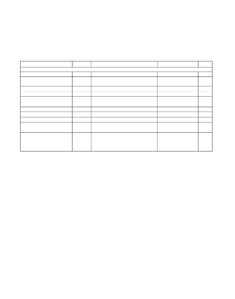
�High-Efficiency,� Low-I� Q� ,� PMICs� with� Dynamic�
�Voltage� Management� for� Mobile� Applications�
�ELECTRICAL� CHARACTERISTICS� (continued)�
�(V� IN� =� V� IN5� =� V� IN67� =� V� IN8� =� 3.6V,� Figure� 3,� T� A� =� -40°C� to� +85°C,� unless� otherwise� noted.� Typical� values� are� at� T� A� =� +25°C.)� (Note� 2)�
�PARAMETER�
�SYMBOL�
�CONDITIONS�
�MIN�
�TYP�
�MAX�
�UNITS�
�I� 2� C�
�TIMING�
�Clock� Frequency�
�f� SCL�
�400�
�kHz�
�Hold� Time� (Repeated)� START�
�Condition�
�CLK� Low� Period�
�CLK� High� Period�
�Set-Up� Time� for� a� Repeated�
�START� Condition�
�DATA� Hold� Time�
�DATA� Set-Up� Time�
�Set-Up� Time� for� STOP� Condition�
�Bus-Free� Time� Between� STOP�
�and� START�
�t� HD;STA�
�t� LOW�
�t� HIGH�
�t� SU;STA�
�t� HD;DAT�
�t� SU;DAT�
�t� SU;STO�
�t� BUF�
�Figure� 8�
�Figure� 8�
�Figure� 9�
�Figure� 9�
�Figure� 8�
�0.6�
�1.3�
�0.6�
�0.6�
�0�
�100�
�0.6�
�1.3�
�μs�
�μs�
�μs�
�μs�
�μs�
�ns�
�μs�
�μs�
�Maximum� Pulse� Width� of� Spikes�
�that� Must� Be� Suppressed� by� the�
�Input� Filter� of� Both� DATA� and�
�50�
�ns�
�CLK� Signals�
�Note� 2:� Limits� are� 100%� production� tested� at� T� A� =� +25°C.� Limits� over� the� operating� temperature� range� are� guaranteed� through� cor-�
�relation� using� statistical� quality� control� (SQC)� methods.�
�Note� 3:� The� dropout� voltage� is� defined� as� V� IN� -� V� OUT� when� V� OUT� is� 100mV� below� the� nominal� value� of� V� OUT� .�
�Note� 4:� Dropout� voltage� (V� DO� )� is� a� function� of� the� p-channel� switch� resistance� (R� P� )� and� the� inductor� resistance� (R� L� ).�
�The� given� values� assume� R� L� =� 50m� ?� for� the� REG1� inductor� and� 67m� ?� for� the� REG2� inductor:�
�V� DO� =� I� LOAD� (R� P� +� R� L� )�
�Note� 5:� The� maximum� output� current� is� guaranteed� by� correlation� to� the� p-channel� current-limit� threshold,� p-channel� on-resistance,�
�n-channel� on-resistance,� oscillator� frequency,� input� voltage� range,� and� output� voltage� range.� The� maximum� output� current�
�in� the� Electrical� Characteristics� table� is� the� worst-case� output� current� for� the� components� shown� in� Figure� 3� over� then� entire�
�specified� range� of� input� and� output� voltage.� More� output� current� may� be� available� when� alternate� components� and� voltage�
�ranges� are� used.� See� the� Step-Down� Converter� Output� Current� section� for� more� information.�
�Note� 6:� Tested� at� 1.4V� default� output� voltage� for� the� MAX8660,� MAX8660A,� and� MAX8661.� Tested� at� 1.15V� default� output� voltage�
�for� the� MAX8660B.�
�Note� 7:� All� output� voltages� are� possible� in� normal� mode.� In� forced-PWM� mode,� the� minimum� output� voltage� is� limited� by� 0.167� x�
�V� IN� .� For� example,� with� V� IN� =� 5.688V,� the� minimum� output� is� 0.95V.�
�10�
�相关PDF资料 |
PDF描述 |
|---|---|
| 462A046-4/86-0 | BOOT MOLDED |
| 0210491091 | CABLE JUMPER 1.25MM .229M 37POS |
| RBC06DRTI-S734 | CONN EDGECARD 12POS DIP .100 SLD |
| H8PPH-2006M | DIP CABLE - HDP20H/AE20M/HDP20H |
| HCC05DRXS-S734 | CONN EDGECARD 10POS DIP .100 SLD |
相关代理商/技术参数 |
参数描述 |
|---|---|
| MAX8660ETL/V+ | 功能描述:PMIC 解决方案 Low-IQ PMIC w/Dynamic V Mgt RoHS:否 制造商:Texas Instruments 安装风格:SMD/SMT 封装 / 箱体:QFN-24 封装:Reel |
| MAX8660ETL/V+T | 功能描述:PMIC 解决方案 Low-IQ PMIC w/Dynamic V Mgt RoHS:否 制造商:Texas Instruments 安装风格:SMD/SMT 封装 / 箱体:QFN-24 封装:Reel |
| MAX8660ETL+ | 功能描述:PMIC 解决方案 Low-IQ PMIC w/Dynamic V Mgt RoHS:否 制造商:Texas Instruments 安装风格:SMD/SMT 封装 / 箱体:QFN-24 封装:Reel |
| MAX8660ETL+T | 功能描述:PMIC 解决方案 Low-IQ PMIC w/Dynamic V Mgt RoHS:否 制造商:Texas Instruments 安装风格:SMD/SMT 封装 / 箱体:QFN-24 封装:Reel |
| MAX8660EVKIT+ | 制造商:Maxim Integrated Products 功能描述:MAX8660 EVAL KIT/EVAL SYS - Rail/Tube |
发布紧急采购,3分钟左右您将得到回复。