- 您现在的位置:买卖IC网 > PDF目录296470 > MAX8795A+ (MAXIM INTEGRATED PRODUCTS INC) 1.6 A SWITCHING REGULATOR, 1400 kHz SWITCHING FREQ-MAX, QCC32 PDF资料下载
参数资料
| 型号: | MAX8795A+ |
| 厂商: | MAXIM INTEGRATED PRODUCTS INC |
| 元件分类: | 稳压器 |
| 英文描述: | 1.6 A SWITCHING REGULATOR, 1400 kHz SWITCHING FREQ-MAX, QCC32 |
| 封装: | 5 X 5 MM, 0.80 MM HEIGHT, LEAD FREE, MO-220WHHD-2, TQFN-32 |
| 文件页数: | 12/24页 |
| 文件大小: | 387K |
| 代理商: | MAX8795A+ |
MAX8795A
TFT-LCD DC-DC Converter with
Operational Amplifiers
2
_
__
_
A
AB
BS
SO
OL
LU
UT
TE
E M
MA
AX
XIIM
MU
UM
M R
RA
AT
TIIN
NG
GS
S
Stresses beyond those listed under “Absolute Maximum Ratings” may cause permanent damage to the device. These are stress ratings only, and functional
operation of the device at these or any other conditions beyond those indicated in the operational sections of the specifications is not implied. Exposure to
absolute maximum rating conditions for extended periods may affect device reliability.
IN, CTL to AGND ...................................................-0.3V to +7.5V
COMP, FB, FBP, FBN, DEL, REF to AGND ....-0.3V to (VIN + 0.3V)
PGND, BGND to AGND ......................................................±0.3V
LX to PGND ............................................................-0.3V to +20V
SUP to AGND .........................................................-0.3V to +20V
DRVP to AGND.......................................................-0.3V to +36V
POS_, NEG_, OUT_ to AGND ...................-0.3V to (VSUP + 0.3V)
DRVN to AGND ...................................(VIN - 30V) to (VIN + 0.3V)
SRC to AGND .........................................................-0.3V to +40V
COM, DRN to AGND ................................-0.3V to (VSRC + 0.3V)
DRN to COM............................................................-30V to +30V
POS_ to NEG_ RMS Current ...................................5mA (Note 1)
OUT_ Maximum Continuous Output Current....................±75mA
LX Switch Maximum Continuous RMS Current .....................1.6A
Continuous Power Dissipation (TA = +70°C)
32-Pin Thin QFN (derate 34.5mW/°C above +70°C) 2758mW
Operating Temperature Range ...........................-40°C to +85°C
Junction Temperature ......................................................+150°C
Storage Temperature Range .............................-65°C to +150°C
Lead Temperature (soldering, 10s) .................................+300°C
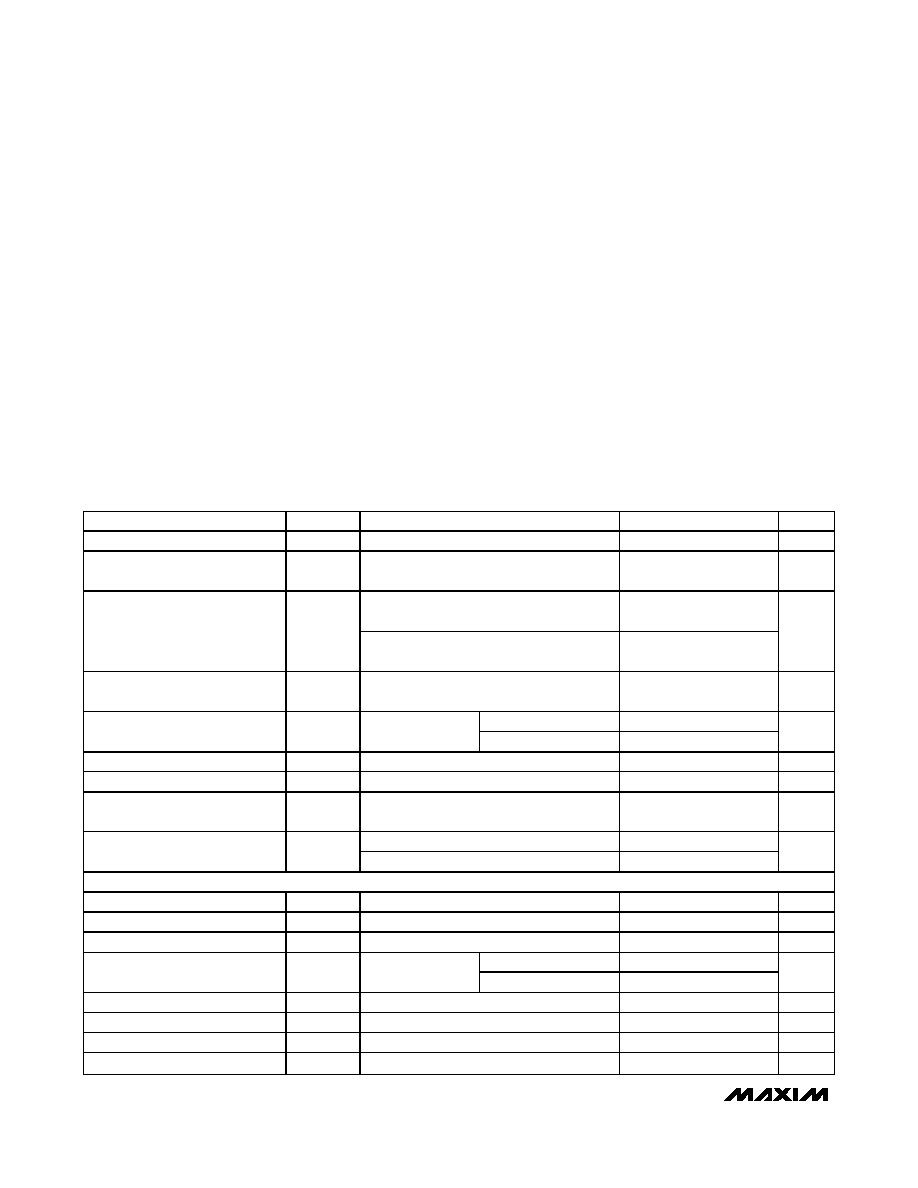
ELECTRICAL CHARACTERISTICS
(VIN = 3V, VMAIN = VSUP = 14V, PGND = AGND = BGND = 0, IREF = 25A, TA = 0°C to +85°C. Typical values are at TA = +25°C,
unless otherwise noted.)
PARAMETER
SYMBOL
CONDITIONS
MIN
TYP
MAX
UNITS
IN Supply Range
VIN
(Note 2)
2.5
6.0
V
IN Undervoltage-Lockout
Threshold
VUVLO
VIN rising, typical hysteresis = 50mV
2.05
2.25
2.45
V
VFB = VFBP = 1.3V, VFBN = 0,
LX not switching
0.6
1.0
IN Quiescent Current
IIN
VFB = 1.2V, VFBP = 1.4V, VFBN = 0,
LX switching
23
mA
Duration to Trigger Fault
Condition
FB or FBP below threshold or FBN above
threshold
200
ms
TA = +25
°C to +85°C
1.238
1.250
1.262
REF Output Voltage
No external load
TA = 0
°C to +85°C
1.232
1.250
1.266
V
REF Load Regulation
0 < ILOAD < 50A
10
mV
REF Sink Current
In regulation
10
A
REF Undervoltage Lockout
Threshold
Rising edge; typical hysteresis = 160mV
1.15
V
Temperature rising
+160
Thermal Shutdown
Hysteresis
15
°C
MAIN STEP-UP REGULATOR
Output Voltage Range
VMAIN
VIN
18
V
Operating Frequency
fOSC
1000
1200
1400
kHz
Oscillator Maximum Duty Cycle
86
90
93
%
TA = +25
°C to +85°C
1.221
1.233
1.245
FB Regulation Voltage
VFB
No load
TA = 0
°C to +85°C
1.212
1.233
1.248
V
FB Fault Trip Level
VFB falling
1.10
1.14
1.17
V
FB Load Regulation
0 < IMAIN < full load, transient only
-1
%
FB Line Regulation
VIN = 2.5V to 6V
0.1
±0.4
%/ V
FB Input Bias Current
VFB = 1.233V
+100
+200
nA
Note 1: See Figure 2 for the op amp clamp structure.
相关PDF资料 |
PDF描述 |
|---|---|
| MAX879CSA | IC LOGIC 16213 24-BIT FET BUS-EXCHANGE SWITCH -40+85C TSSOP-56 1500/REEL |
| MAX9851EVCMODU | MAX9851评估板/评估系统 |
| MAX9934FART+T | SPECIALTY ANALOG CIRCUIT, PBGA6 |
| MAX9950FCCB | SPECIALTY ANALOG CIRCUIT, PQFP64 |
| MAX9966BGCCQ+D | Quad, Low-Power, 500Mbps ATE Driver/Comparator |
相关代理商/技术参数 |
参数描述 |
|---|---|
| MAX8795AETJ+ | 功能描述:直流/直流开关转换器 TFT-LCD DC/DC Converter RoHS:否 制造商:STMicroelectronics 最大输入电压:4.5 V 开关频率:1.5 MHz 输出电压:4.6 V 输出电流:250 mA 输出端数量:2 最大工作温度:+ 85 C 安装风格:SMD/SMT |
| MAX8795AETJ+C7P | 功能描述:显示驱动器和控制器 TFT-LCD DC/DC Converter RoHS:否 制造商:Panasonic Electronic Components 工作电源电压:2.7 V to 5.5 V 最大工作温度: 安装风格:SMD/SMT 封装 / 箱体:QFN-44 封装:Reel |
| MAX8795AETJ+T | 功能描述:LCD 驱动器 TFT-LCD DC/DC Converter RoHS:否 制造商:Maxim Integrated 数位数量:4.5 片段数量:30 最大时钟频率:19 KHz 工作电源电压:3 V to 3.6 V 最大工作温度:+ 85 C 最小工作温度:- 20 C 封装 / 箱体:PDIP-40 封装:Tube |
| MAX8795AEVKIT+ | 功能描述:电源管理IC开发工具 MAX8795A Eval Kit RoHS:否 制造商:Maxim Integrated 产品:Evaluation Kits 类型:Battery Management 工具用于评估:MAX17710GB 输入电压: 输出电压:1.8 V |
| MAX8795AGCJ/V+ | 功能描述:LCD 驱动器 TFT-LCD DC/DC Converter RoHS:否 制造商:Maxim Integrated 数位数量:4.5 片段数量:30 最大时钟频率:19 KHz 工作电源电压:3 V to 3.6 V 最大工作温度:+ 85 C 最小工作温度:- 20 C 封装 / 箱体:PDIP-40 封装:Tube |
发布紧急采购,3分钟左右您将得到回复。