- 您现在的位置:买卖IC网 > PDF目录5136 > MAX8795AGCJ+T (Maxim Integrated Products)IC CONV DC-DC TFT-LCD 32LQFP PDF资料下载
参数资料
| 型号: | MAX8795AGCJ+T |
| 厂商: | Maxim Integrated Products |
| 文件页数: | 13/31页 |
| 文件大小: | 0K |
| 描述: | IC CONV DC-DC TFT-LCD 32LQFP |
| 产品培训模块: | Lead (SnPb) Finish for COTS Obsolescence Mitigation Program |
| 标准包装: | 2,000 |
| 应用: | 转换器,TFT,LCD |
| 输入电压: | 2.5 V ~ 6 V |
| 输出数: | 8 |
| 输出电压: | 2.5 V ~ 18 V |
| 工作温度: | -40°C ~ 105°C |
| 安装类型: | 表面贴装 |
| 封装/外壳: | 32-LQFP |
| 供应商设备封装: | 32-LQFP(7x7) |
| 包装: | 带卷 (TR) |
第1页第2页第3页第4页第5页第6页第7页第8页第9页第10页第11页第12页当前第13页第14页第15页第16页第17页第18页第19页第20页第21页第22页第23页第24页第25页第26页第27页第28页第29页第30页第31页
�� �
�
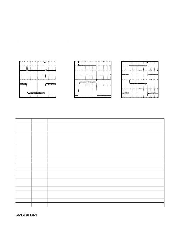
�TFT-LCD� DC-DC� Converter� with�
�Operational� Amplifiers�
�Typical� Operating� Characteristics� (continued)�
�(Circuit� of� Figure� 1,� V� IN� =� 5V,� V� MAIN� =� 14V,� V� GON� =� 25V,� V� GOFF� =� -10V,� T� A� =� +25°C,� unless� otherwise� noted.)�
�OPERATIONAL-AMPLIFIER�
�LOAD-TRANSIENT� RESPONSE�
�MAX8795A� toc15�
�A�
�OPERATIONAL-AMPLIFIER�
�LARGE-SIGNAL� RESPONSE�
�MAX8795A� toc16�
�V� SUP� = 15V�
�OPERATIONAL-AMPLIFIER�
�SMALL-SIGNAL� RESPONSE�
�MAX8795A� toc17�
�0V�
�A�
�A�
�0V�
�0V�
�+50mA�
�400ns/div�
�A:� OUTPUT� VOLTAGE,� 1V/div,� AC-COUPLED�
�B:� OUTPUT� CURRENT,� 50mA/div�
�B�
�0mA�
�-50mA�
�1� μ� s/div�
�A:� INPUT� SIGNAL,� 5V/div�
�B:� OUTPUT� SIGNAL,� 5V/div�
�B�
�0V�
�B�
�0V�
�400ns/div�
�A:� INPUT� SIGNAL,� 100mV/div�
�B:� OUTPUT� SIGNAL,� 100mV/div�
�Pin� Description�
�PIN�
�1�
�2�
�3�
�4�
�5�
�6�
�7�
�8�
�9�
�10�
�11�
�12�
�13�
�14�
�15�
�16�
�NAME�
�SRC�
�REF�
�AGND�
�PGND�
�OUT1�
�NEG1�
�POS1�
�OUT2�
�NEG2�
�POS2�
�BGND�
�POS3�
�OUT3�
�SUP�
�POS4�
�NEG4�
�FUNCTION�
�Switch� Input.� Source� of� the� internal� high-voltage� p-channel� MOSFET.� Bypass� SRC� to� PGND� with� a�
�minimum� 0.1μF� capacitor� close� to� the� pins.�
�Reference� Bypass� Terminal.� Bypass� REF� to� AGND� with� a� minimum� of� 0.22μF� close� to� the� pins.�
�Analog� Ground� for� Step-Up� Regulator� and� Linear� Regulators.� Connect� to� power� ground� (PGND)�
�underneath� the� IC.�
�Power� Ground.� PGND� is� the� source� of� the� main� step-up� n-channel� power� MOSFET.� Connect� PGND� to�
�the� output-capacitor� ground� terminals� through� a� short,� wide� PCB� trace.� Connect� to� analog� ground�
�(AGND)� underneath� the� IC.�
�Operational-Amplifier� 1� Output�
�Operational-Amplifier� 1� Inverting� Input�
�Operational-Amplifier� 1� Noninverting� Input�
�Operational-Amplifier� 2� Output�
�Operational-Amplifier� 2� Inverting� Input�
�Operational-Amplifier� 2� Noninverting� Input�
�Analog� Ground� for� Operational� Amplifiers.� Connect� to� power� ground� (PGND)� underneath� the� IC.�
�Operational-Amplifier� 3� Noninverting� Input�
�Operational-Amplifier� 3� Output�
�Operational-Amplifier� Power� Input.� Positive� supply� rail� for� the� operational� amplifiers.� Typically�
�connected� to� V� MAIN� .� Bypass� SUP� to� BGND� with� a� 0.1μF� capacitor.�
�Operational-Amplifier� 4� Noninverting� Input�
�Operational-Amplifier� 4� Inverting� Input�
�______________________________________________________________________________________�
�13�
�相关PDF资料 |
PDF描述 |
|---|---|
| MAX606ESA+ | IC DC-DC CONVERT 8-SOIC |
| RBC18DRSD-S273 | CONN EDGECARD 36POS DIP .100 SLD |
| X40430S14-C | IC VOLT MON TRPL EEPROM 14-SOIC |
| X40430S14-BT1 | IC VOLT MON TRPL EEPROM 14-SOIC |
| X40430S14-B | IC VOLT MON TRPL EEPROM 14-SOIC |
相关代理商/技术参数 |
参数描述 |
|---|---|
| MAX8796GTJ+ | 功能描述:电压模式 PWM 控制器 IMVP6 Single-Phase PWM Controller RoHS:否 制造商:Texas Instruments 输出端数量:1 拓扑结构:Buck 输出电压:34 V 输出电流: 开关频率: 工作电源电压:4.5 V to 5.5 V 电源电流:600 uA 最大工作温度:+ 125 C 最小工作温度:- 40 C 封装 / 箱体:WSON-8 封装:Reel |
| MAX8796GTJ+C8V | 制造商:Maxim Integrated Products 功能描述:IMVP6/GMCH CONTROLLER - Rail/Tube |
| MAX8796GTJ+G05 | 制造商:Maxim Integrated Products 功能描述:IMVP6/GMCH CONTROLLER - Rail/Tube |
| MAX8796GTJ+G071 | 制造商:Maxim Integrated Products 功能描述:IMVP6/GMCH CONTROLLER - Rail/Tube |
| MAX8796GTJ+G1D | 功能描述:电压模式 PWM 控制器 1-Phase Quick-PWM Intel IMVP-6/GMCH RoHS:否 制造商:Texas Instruments 输出端数量:1 拓扑结构:Buck 输出电压:34 V 输出电流: 开关频率: 工作电源电压:4.5 V to 5.5 V 电源电流:600 uA 最大工作温度:+ 125 C 最小工作温度:- 40 C 封装 / 箱体:WSON-8 封装:Reel |
发布紧急采购,3分钟左右您将得到回复。