- 您现在的位置:买卖IC网 > PDF目录10644 > MAX912ESE+T (Maxim Integrated Products)IC COMPARATOR LP 16-SOIC PDF资料下载
参数资料
| 型号: | MAX912ESE+T |
| 厂商: | Maxim Integrated Products |
| 文件页数: | 4/11页 |
| 文件大小: | 0K |
| 描述: | IC COMPARATOR LP 16-SOIC |
| 产品培训模块: | Lead (SnPb) Finish for COTS Obsolescence Mitigation Program |
| 标准包装: | 2,500 |
| 类型: | 带锁销 |
| 元件数: | 2 |
| 输出类型: | 补充型,TTL |
| 电压 - 电源,单路/双路(±): | 5 V ~ 10 V |
| 电压 - 输入偏移(最小值): | 2mV @ ±5V |
| 电流 - 输入偏压(最小值): | 5µA @ ±5V |
| 电流 - 输出(标准): | 20mA |
| 电流 - 静态(最大值): | 10mA |
| CMRR, PSRR(标准): | 110dB CMRR,100dB PSRR |
| 传输延迟(最大): | 14ns |
| 工作温度: | -40°C ~ 85°C |
| 封装/外壳: | 16-SOIC(0.154",3.90mm 宽) |
| 安装类型: | 表面贴装 |
| 包装: | 带卷 (TR) |
MAX912/MAX913
Single/Dual, Ultra-Fast, Low-Power
Precision TTL Comparators
2
_______________________________________________________________________________________
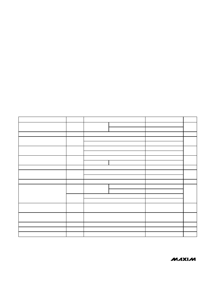
ABSOLUTE MAXIMUM RATINGS
ELECTRICAL CHARACTERISTICS
V+ = +5V, V- = -5V, VQ = 1.4V, VLE = 0V, TA = TMIN to TMAX, unless otherwise noted. Typical values are at TA = +25°C.) (Note 1)
Stresses beyond those listed under “Absolute Maximum Ratings” may cause permanent damage to the device. These are stress ratings only, and functional
operation of the device at these or any other conditions beyond those indicated in the operational sections of the specifications is not implied. Exposure to
absolute maximum rating conditions for extended periods may affect device reliability.
Positive Supply Voltage .........................................................+7V
Negative Supply Voltage ........................................................-7V
V+ to V- ................................................................................+13V
Differential Input Voltage .....................................................+15V
Input Voltage (Referred to V-) ................................-0.3V to +14V
Latch Pin Voltage .............................................Equal to Supplies
Continuous Output Current...............................................±20mA
Continuous Power Dissipation (TA = +70°C)
8-Pin Plastic DIP (derate 9.09mW/°C above +70°C) ...727mW
8-Pin SO (derate 5.88mW/°C above +70°C)................471mW
8-Pin MAX (derate 4.5mW/°C above +70°C) .............362mW
16-Pin Plastic DIP (derate 10.53mW/°C above +70°C)842mW
16-Pin Narrow SO (derate 8.70mW/°C above +70°C) .696mW
Operating Temperature Ranges:
MAX91_C_ _ ...........................................................0°C to +70°C
MAX91_E_ _.........................................................-40°C to +85°C
Storage Temperature Range .............................-65°C to +150°C
Lead Temperature (soldering, 10s) .................................+300°C
PARAMETER
SYMBOL
CONDITIONS
MIN
TYP
MAX
UNITS
TA = +25°C
0.1
2
Input Offset Voltage (Note 2)
VOS
RS
≤ 100
TA = TMIN TO TMAX
3
mV
Offset Drift
TCVOS
2
V/°C
TA = +25°C
0.3
0.5
Input Offset Current (Note 2)
IOS
TA = TMIN TO TMAX
1
A
TA = +25°C2
5
Input Bias Current
IB
C, E temperature ranges
8
A
C, E temperature ranges
-5.2
+3.5
Input Voltage Range
VCM
Single +5V
C, E temperature ranges
-0.2
+3.5
V
Common-Mode Rejection Ratio
CMRR
-5.0V
≤ VCM ≤ +3.5V
80
110
dB
Positive supply; 4.5V
≤ V+ ≤ 5.5V
60
85
Power-Supply Rejection Ratio
PSRR
Negative supply; -2V
≥ V- ≥ -7V
80
100
dB
Small-Signal Voltage Gain
AV
1V
≤ VQ ≤ 2V, TA = +25°C
1500
3500
V/V
IOUT = 1mA
2.7
3.4
VOH
V+
≥ 4.5V
IOUT = 10mA
2.4
3.0
ISINK = 4mA
0.3
0.5
Output Voltage
VOL
TA = +25°C, ISINK = 10mA
0.4
V
Positive Supply Current Per
Comparator (Note 3)
I+
C, E temperature ranges
6
10
mA
Negative Supply Current Per
Comparator (Note 3)
I-
1
2
mA
Latch-Pin High Input Voltage
VIH
2.0
V
Latch-Pin Low Input Voltage
VIL
0.8
V
Latch-Pin Current
IIL
VLE = 0V
-1
-20
A
相关PDF资料 |
PDF描述 |
|---|---|
| VI-J50-MY-F1 | CONVERTER MOD DC/DC 5V 50W |
| MAX901BCSE+T | IC COMPARATOR VOLT 16-SOIC |
| MAX9111EKA+T | IC RCVR LVDS SGL SOT23-8 |
| VE-JTL-MY-F4 | CONVERTER MOD DC/DC 28V 50W |
| VE-JTL-MY-F3 | CONVERTER MOD DC/DC 28V 50W |
相关代理商/技术参数 |
参数描述 |
|---|---|
| MAX912MJE | 功能描述:校验器 IC RoHS:否 制造商:STMicroelectronics 产品: 比较器类型: 通道数量: 输出类型:Push-Pull 电源电压-最大:5.5 V 电源电压-最小:1.1 V 补偿电压(最大值):6 mV 电源电流(最大值):1350 nA 响应时间: 最大工作温度:+ 125 C 安装风格:SMD/SMT 封装 / 箱体:SC-70-5 封装:Reel |
| MAX913 | 制造商:MAXIM 制造商全称:Maxim Integrated Products 功能描述:Single/Dual, Ultra-Fast, Low-Power, Precision TTL Comparators |
| MAX9130 | 制造商:MAXIM 制造商全称:Maxim Integrated Products 功能描述:Single 500Mbps LVDS Line Receiver in SC70 |
| MAX9130EXT | 制造商:Maxim Integrated Products 功能描述:SINGLE 500MBPS LVDS LINE RECEIVER I - Cut Tape Product |
| MAX9130EXT+ | 制造商:Maxim Integrated Products 功能描述:LINE RCVR 1RX 6PIN SC-70 - Rail/Tube |
发布紧急采购,3分钟左右您将得到回复。