- 您现在的位置:买卖IC网 > PDF目录11677 > MAX9205EAI/V+ (Maxim Integrated Products)IC SERIALIZER BUS/LVDS 28SSOP PDF资料下载
参数资料
| 型号: | MAX9205EAI/V+ |
| 厂商: | Maxim Integrated Products |
| 文件页数: | 6/13页 |
| 文件大小: | 0K |
| 描述: | IC SERIALIZER BUS/LVDS 28SSOP |
| 其它有关文件: | Automotive Product Guide |
| 产品培训模块: | Lead (SnPb) Finish for COTS Obsolescence Mitigation Program |
| 标准包装: | 46 |
| 功能: | 串行器 |
| 数据速率: | 400Mbps |
| 输入类型: | LVTTL/LVCMOS |
| 输出类型: | LVDS |
| 输入数: | 10 |
| 输出数: | 1 |
| 电源电压: | 3 V ~ 3.6 V |
| 工作温度: | -40°C ~ 85°C |
| 安装类型: | 表面贴装 |
| 封装/外壳: | 28-SSOP(0.209",5.30mm 宽) |
| 供应商设备封装: | 28-SSOP |
| 包装: | 管件 |
MAX9205/MAX9207
10-Bit Bus LVDS Serializers
2
Maxim Integrated
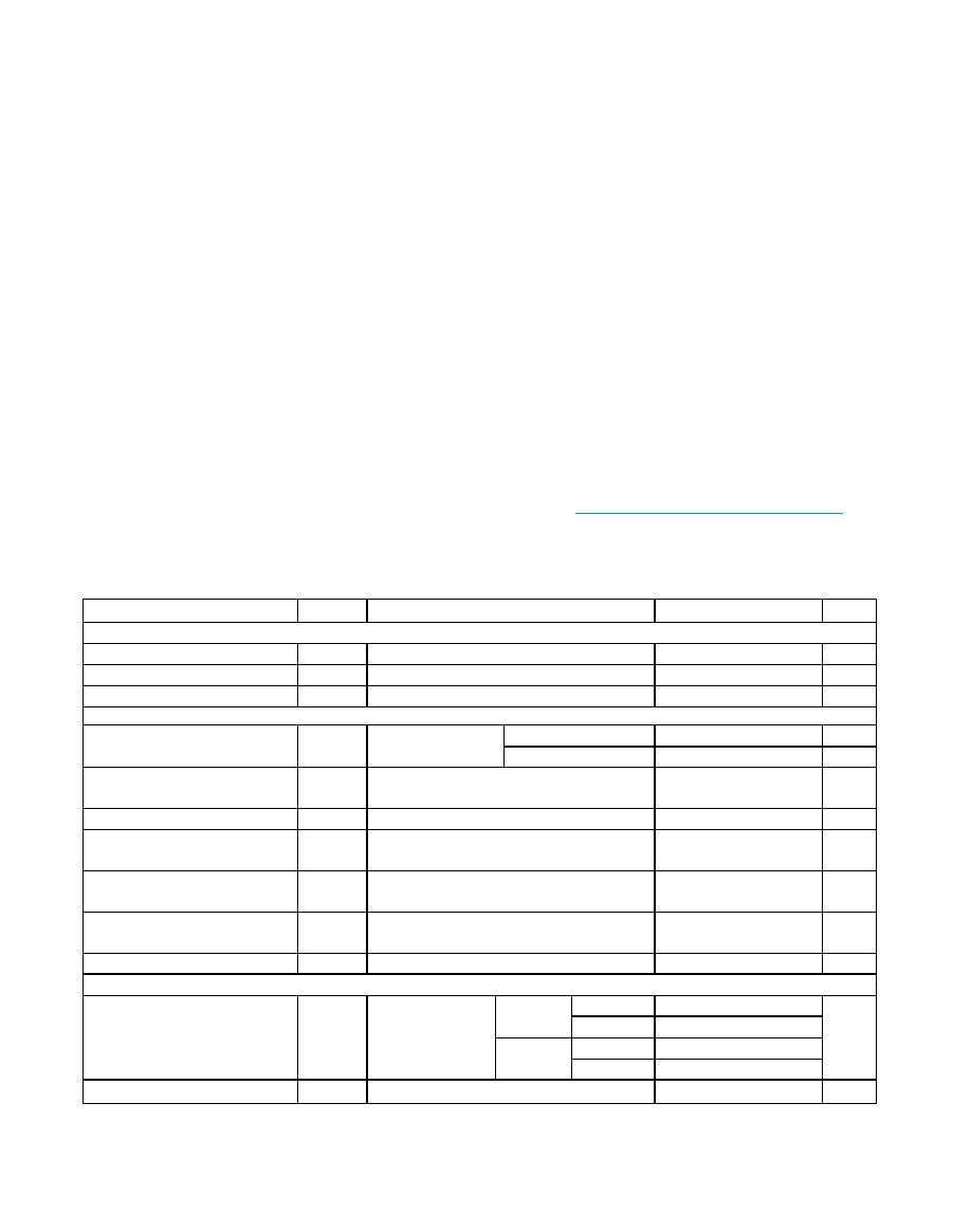
ABSOLUTE MAXIMUM RATINGS
DC ELECTRICAL CHARACTERISTICS
(VAVCC = VDVCC = +3.0V to +3.6V, RL = 27 ±1% or 50 ±1%, CL = 10pF, TA = -40°C to +85°C. Typical values are at VAVCC =
VDVCC = +3.3V and TA = +25°C, unless otherwise noted.) (Notes 2, 3, 4)
Stresses beyond those listed under “Absolute Maximum Ratings” may cause permanent damage to the device. These are stress ratings only, and functional
operation of the device at these or any other conditions beyond those indicated in the operational sections of the specifications is not implied. Exposure to
absolute maximum rating conditions for extended periods may affect device reliability.
AVCC, DVCC to GND..........................……………-0.3V to +4.0V
IN_, SYNC1, SYNC2, EN, TCLK_R/F, TCLK,
PWRDN to GND......................................-0.3V to (VCC + 0.3V)
OUT+, OUT- to GND .............................................-0.3V to +4.0V
Output Short-Circuit Duration.....................................Continuous
Continuous Power Dissipation (TA = +70°C)
28-Pin SSOP (derate 9.5mW/°C above +70°C) ..........762mW
Storage Temperature Range .............................-65°C to +150°C
Junction Temperature ......................................................+150°C
Operating Temperature Range ...........................-40°C to +85°C
ESD Protection (Human Body Model, OUT+, OUT-) ...........±8kV
Lead Temperature (soldering, 10s) .................................+300°C
Soldering Temperature (reflow) .......................................+260°C
PARAMETER
SYMBOL
CONDITIONS
MIN
TYP
MAX
UNITS
LVCMOS/LVTLL LOGIC INPUTS (IN0 TO IN9, EN, SYNC1, SYNC2, TCLK, TCLK_R/
F, PWRDN)
High-Level Input Voltage
VIH
2.0
VCC
V
Low-Level Input Voltage
VIL
GND
0.8
V
Input Current
IIN
VIN_ = 0V or V_VCC
-20
+20
A
BUS LVDS OUTPUTS (OUT+, OUT-)
RL = 27
200
286
400
mV
Differential Output Voltage
VOD
Figure 1
RL = 50
250
460
600
mV
Change in VOD Between
Complementary Output States
VOD
Figure 1
1
35
mV
Output Offset Voltage
VOS
Figure 1
0.9
1.15
1.3
V
Change in VOS Between
Complementary Output States
VOS
Figure 1
3
35
mV
Output Short-Circuit Current
IOS
VOUT+ or VOUT- = 0V,
IN0 to IN9 =
PWRDN = EN = high
-13
-15
mA
Output High-Impedance Current
IOZ
VPWRDN or VEN = 0.8V,
VOUT+ or VOUT- = 0V or V_VCC
-10
+10
A
Power-Off Output Current
IOX
V_VCC = 0V, VOUT+ or VOUT- = 0V or 3.6V
-10
+10
A
POWER SUPPLY
16MHz
23
35
MAX9205
40MHz
34
45
40MHz
32
50
Supply Current
ICC
RL = 27_ or 50_
worst-case pattern
(Figures 2, 4)
MAX9207
66MHz
45
60
mA
Power-Down Supply Current
ICCX
PWRDN = low
8
mA
Note 1: Package thermal resistances were obtained using the method described in JEDEC specification JESD51-7, using a four-layer
board. For detailed information on package thermal considerations, refer to www.maximintegrated.com/thermal-tutorial.
PACKAGE THERMAL CHARACTERISTICS (Note 1)
SSOP
Junction-to-Ambient Thermal Resistance (
θJA)...............68°C/W
Junction-to-Case Thermal Resistance (
θJC)......................25°C/W
相关PDF资料 |
PDF描述 |
|---|---|
| VI-BVM-IX-F3 | CONVERTER MOD DC/DC 10V 75W |
| CONN012 | CONN N-MALE R/A END CRIMP RG-174 |
| MS27497E18A66S | CONN RCPT 66POS WALL MNT W/SCKT |
| CONN007 | CONN N-MALE END CRIMP RG-174 |
| D38999/20KB5SN | CONN RCPT 5POS WALL MNT W/SCKT |
相关代理商/技术参数 |
参数描述 |
|---|---|
| MAX9205EAV | 制造商:MAXIM 制造商全称:Maxim Integrated Products 功能描述:10-Bit Bus LVDS Serializers |
| MAX9205EVKIT | 制造商:Maxim Integrated Products 功能描述:10-BIT BUS LVDS SERIALIZER - Bulk |
| MAX9206 | 制造商:MAXIM 制造商全称:Maxim Integrated Products 功能描述:10-Bit Bus LVDS Deserializers |
| MAX9206_07 | 制造商:MAXIM 制造商全称:Maxim Integrated Products 功能描述:10-Bit Bus LVDS Deserializers |
| MAX9206_10 | 制造商:MAXIM 制造商全称:Maxim Integrated Products 功能描述:10-Bit Bus LVDS Deserializers |
发布紧急采购,3分钟左右您将得到回复。