- 您现在的位置:买卖IC网 > PDF目录11677 > MAX9205EAI/V+ (Maxim Integrated Products)IC SERIALIZER BUS/LVDS 28SSOP PDF资料下载
参数资料
| 型号: | MAX9205EAI/V+ |
| 厂商: | Maxim Integrated Products |
| 文件页数: | 9/13页 |
| 文件大小: | 0K |
| 描述: | IC SERIALIZER BUS/LVDS 28SSOP |
| 其它有关文件: | Automotive Product Guide |
| 产品培训模块: | Lead (SnPb) Finish for COTS Obsolescence Mitigation Program |
| 标准包装: | 46 |
| 功能: | 串行器 |
| 数据速率: | 400Mbps |
| 输入类型: | LVTTL/LVCMOS |
| 输出类型: | LVDS |
| 输入数: | 10 |
| 输出数: | 1 |
| 电源电压: | 3 V ~ 3.6 V |
| 工作温度: | -40°C ~ 85°C |
| 安装类型: | 表面贴装 |
| 封装/外壳: | 28-SSOP(0.209",5.30mm 宽) |
| 供应商设备封装: | 28-SSOP |
| 包装: | 管件 |
MAX9205/MAX9207
10-Bit Bus LVDS Serializers
5
Maxim Integrated
Pin Description
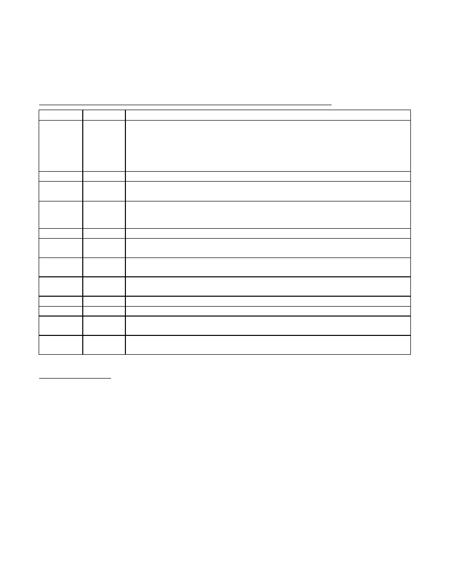
PIN
NAME
FUNCTION
1, 2
SYNC 1,
SYNC 2
LVCMOS/LVTTL Logic Inputs. The two SYNC pins are ORed. When at least one of the two pins
are asserted high for at least six cycles of TCLK, the serializer initiates a transmission of 1024
SYNC patterns. If held high after 1024 SYNC patterns have been transmitted, SYNC patterns
continue to be sent until the SYNC pin is asserted low. Toggling a SYNC pin after six TCLK cycles
high and before 1024 SYNC patterns have been transmitted does not affect the output of the 1024
SYNC patterns.
3–12
IN0–IN9
LVCMOS/LVTTL Data Inputs. Data is loaded into a 10-bit latch by the selected TCLK edge.
13
TCLK_R/
F
LVCMOS/LVTTL Logic Input. High selects a TCLK rising-edge data strobe. Low selects a TCLK
falling-edge data strobe.
14
TCLK
LVCMOS/LVTTL Reference Clock Input. The MAX9205 accepts a 16MHz to 40MHz clock. The
MAX9207 accepts a 40MHz to 66MHz clock. TCLK provides a frequency reference to the PLL and
strobes parallel data into the input latch.
15, 16
DGND
Digital Circuit Ground. Connect to ground plane.
17, 26
AVCC
Analog Circuit Power Supply (Includes PLL). Bypass AVCC to ground with a 0.1F capacitor and a
0.001F capacitor. Place the 0.001F capacitor closest to AVCC.
18, 20,
23, 25
AGND
Analog Circuit Ground. Connect to ground plane.
19
EN
LVCMOS/LVTTL Logic Input. High enables serial data output. Low puts the bus LVDS output into
high impedance.
21
OUT-
Inverting Bus LVDS Differential Output
22
OUT+
Noninverting Bus LVDS Differential Output
24
PWRDN
LVCMOS/LVTTL Logic Input. Low puts the device into power-down mode and the output into high
impedance.
27, 28
DVCC
Digital Circuit Power Supply. Bypass DVCC to ground with a 0.1F capacitor and a 0.001F
capacitor. Place the 0.001F capacitor closest to DVCC.
Detailed Description
The MAX9205/MAX9207 are 10-bit serializers designed
to transmit data over balanced media that may be a
standard twisted-pair cable or PCB traces at 160Mbps
to 660Mbps. The interface may be double-terminated
point-to-point or a heavily loaded multipoint bus. The
characteristic impedance of the media and connected
devices can range from 100
for a point-to-point inter-
face to 54
for a heavily loaded multipoint bus. A dou-
ble-terminated point-to-point interface uses a
100
-termination resistor at each end of the interface,
resulting in a load of 50
. A heavily loaded multipoint
bus requires a termination as low as 54
at each end
of the bus, resulting in a termination load of 27
. The
serializer requires a deserializer such as the
MAX9206/MAX9208 for a complete data transmission
application.
A high-state start bit and a low-state stop bit, added
internally, frame the 10-bit parallel input data and
ensure a transition in the serial data stream. Therefore,
12 serial bits are transmitted for each 10-bit parallel
input. The MAX9205 accepts a 16MHz to 40MHz refer-
ence clock, producing a serial data rate of 192Mbps
(12 bits x 16MHz) to 480Mbps (12 bits x 40MHz). The
MAX9207 accepts a 40MHz to 66MHz reference clock,
producing 480Mbps to 792Mbps. However, since only
10 bits are from input data, the actual throughput is 10
times the TCLK frequency.
To transmit data, the serializers sequence through
three modes: initialization mode, synchronization mode,
and data transmission mode.
相关PDF资料 |
PDF描述 |
|---|---|
| VI-BVM-IX-F3 | CONVERTER MOD DC/DC 10V 75W |
| CONN012 | CONN N-MALE R/A END CRIMP RG-174 |
| MS27497E18A66S | CONN RCPT 66POS WALL MNT W/SCKT |
| CONN007 | CONN N-MALE END CRIMP RG-174 |
| D38999/20KB5SN | CONN RCPT 5POS WALL MNT W/SCKT |
相关代理商/技术参数 |
参数描述 |
|---|---|
| MAX9205EAV | 制造商:MAXIM 制造商全称:Maxim Integrated Products 功能描述:10-Bit Bus LVDS Serializers |
| MAX9205EVKIT | 制造商:Maxim Integrated Products 功能描述:10-BIT BUS LVDS SERIALIZER - Bulk |
| MAX9206 | 制造商:MAXIM 制造商全称:Maxim Integrated Products 功能描述:10-Bit Bus LVDS Deserializers |
| MAX9206_07 | 制造商:MAXIM 制造商全称:Maxim Integrated Products 功能描述:10-Bit Bus LVDS Deserializers |
| MAX9206_10 | 制造商:MAXIM 制造商全称:Maxim Integrated Products 功能描述:10-Bit Bus LVDS Deserializers |
发布紧急采购,3分钟左右您将得到回复。