- 您现在的位置:买卖IC网 > PDF目录11699 > MAX9209EUM+D (Maxim Integrated Products)IC SERIALIZER PROG 48-TSSOP PDF资料下载
参数资料
| 型号: | MAX9209EUM+D |
| 厂商: | Maxim Integrated Products |
| 文件页数: | 11/18页 |
| 文件大小: | 0K |
| 描述: | IC SERIALIZER PROG 48-TSSOP |
| 其它有关文件: | Automotive Product Guide |
| 产品培训模块: | Lead (SnPb) Finish for COTS Obsolescence Mitigation Program |
| 标准包装: | 39 |
| 功能: | 串行器 |
| 数据速率: | 1.785Gbps |
| 输入类型: | LVTTL/LVCMOS |
| 输出类型: | LVDS |
| 输入数: | 21 |
| 输出数: | 3 |
| 电源电压: | 3 V ~ 3.6 V |
| 工作温度: | -40°C ~ 85°C |
| 安装类型: | 表面贴装 |
| 封装/外壳: | 48-TFSOP(0.240",6.10mm 宽) |
| 供应商设备封装: | 48-TSSOP |
| 包装: | 管件 |
MAX9209/MAX9213
Programmable DC-Balanced
21-Bit Serializers
2
_______________________________________________________________________________________
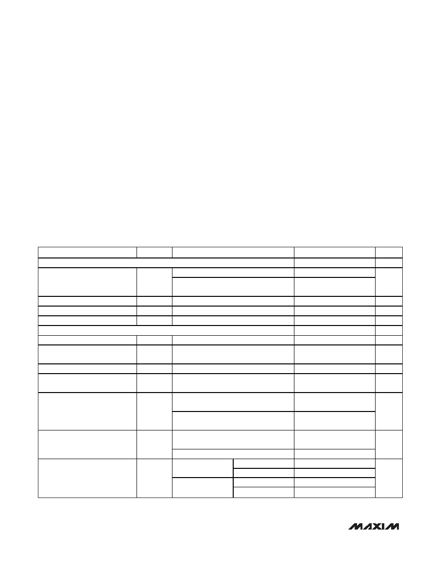
ABSOLUTE MAXIMUM RATINGS
DC ELECTRICAL CHARACTERISTICS
(VCC = +3.0V to +3.6V, RL = 100
±1%, PWRDWN = high, DCB/NC = high or low, unless otherwise noted. Typical values are at VCC
= +3.3V, TA = +25
°C.) (Notes 1, 2)
Stresses beyond those listed under “Absolute Maximum Ratings” may cause permanent damage to the device. These are stress ratings only, and functional
operation of the device at these or any other conditions beyond those indicated in the operational sections of the specifications is not implied. Exposure to
absolute maximum rating conditions for extended periods may affect device reliability.
VCC to GND ...........................................................-0.5V to +4.0V
LVDS Outputs (TxOUT_, TxCLK OUT_) to GND ...-0.5V to +4.0V
5V Tolerant LVTTL/LVCMOS Inputs
(TxIN_, TxCLK IN, PWRDWN) to GND ..............-0.5V to +6.0V
(DCB/NC) to GND ......................................-0.5V to (VCC + 0.5V)
LVDS Outputs (TxOUT_, TxCLK OUT_)
Short to GND and Differential Short .......................Continuous
Continuous Power Dissipation (multilayer board, TA = +70°C)
48-Pin TSSOP (derate 16mW/°C above +70°C) ....... 1282mW
48-Pin TQFN (derate 40mW/°C above +70°C) ..........3200mW
Storage Temperature Range .............................-65°C to +150°C
Junction Temperature ......................................................+150°C
ESD Protection
Human Body Model (RD = 1.5k
, CS = 100pF)
All Pins to GND..............................................................
±2kV
IEC 61000-4-2 (RD = 330
, CS = 150pF)
Contact Discharge (TxOUT_, TxCLK OUT_) to GND ....
±8kV
Air Gap Discharge (TxOUT_, TxCLK OUT_) to GND ..
±15kV
ISO 10605 (RD = 2k
, CS = 330pF)
Contact Discharge (TxOUT_, TxCLK OUT_) to GND ....
±8kV
Air Gap Discharge (TxOUT_, TxCLK OUT_) to GND ..
±25kV
Lead Temperature (soldering, 10s) .................................+300°C
Soldering Temperature (reflow) .......................................+260°C
PARAMETER
SYMBOL
CONDITIONS
MIN
TYP
MAX
UNITS
SINGLE-ENDED INPUTS (TxIN_, TxCLK IN,
PWRDWN, DCB/NC)
TxIN_, TxCLK IN, PWRDWN
2.0
5.5
High-Level Input Voltage
VIH
DCB/NC
2.0
VCC +
0.3
V
Low-Level Input Voltage
VIL
-0.3
+0.8
V
Input Current
IIN
VIN = high or low, PWRDWN = high or low
-20
+20
A
Input Clamp Voltage
VCL
ICL = -18mA
-0.9
-1.5
V
LVDS OUTPUTS (TxOUT_, TxCLK OUT)
Differential Output Voltage
VOD
Figure 1
250
350
450
mV
Change in VOD Between
Complementary Output States
VOD
Figure 1
2
25
mV
Output Offset Voltage
VOS
Figure 1
1.125
1.25
1.375
V
Change in VOS Between
Complementary Output States
VOS
Figure 1
10
30
mV
VOUT+ or VOUT- = 0V or VCC,
non-DC-balanced mode
-10
±5.7
+10
Output Short-Circuit Current
IOS
VOUT+ or VOUT- = 0V or VCC,
DC-balanced mode
-15
±8.2
+15
mA
VOD = 0V, non-DC-balanced mode
(Note 3)
5.7
10
Magnitude of Differential Output
Short-Circuit Current
IOSD
VOD = 0V, DC-balanced mode (Note 3)
8.2
15
mA
78
110
147
DC-balanced mode
-40°C to +105°C
78
110
150
292
410
547
Differential Output Resistance
RO
Non-DC-balanced
mode
-40°C to +105°C
292
410
564
相关PDF资料 |
PDF描述 |
|---|---|
| MAX9234EUM+D | IC DESERIALIZER 21BIT 48TSSOP |
| MAX9273GTL+ | IC GMSL SERIALIZER |
| R5F100CCALA#U0 | MCU 16BIT 32KB FLASH 36FLGA |
| R5F101JCAFA#V0 | MCU 16BIT 32KB FLASH 52LQFP |
| R5F100BDANA#U0 | MCU 16BIT 48KB FLASH 32WQFN |
相关代理商/技术参数 |
参数描述 |
|---|---|
| MAX9209EVKIT+ | 功能描述:界面开发工具 MAX9209/44 Eval Kit RoHS:否 制造商:Bourns 产品:Evaluation Boards 类型:RS-485 工具用于评估:ADM3485E 接口类型:RS-485 工作电源电压:3.3 V |
| MAX9209GUM | 制造商:MAXIM 制造商全称:Maxim Integrated Products 功能描述:Programmable DC-Balanced 21-Bit Serializers |
| MAX9209GUM+ | 制造商:MAXIM 制造商全称:Maxim Integrated Products 功能描述:Programmable DC-Balanced 21-Bit Serializers |
| MAX9209GUM+D | 功能描述:串行器/解串器 - Serdes 21-Bit Bus LVDS Serializer RoHS:否 制造商:Texas Instruments 类型:Deserializer 数据速率:1.485 Gbit/s 输入类型:ECL/LVDS 输出类型:LVCMOS 输入端数量:1 输出端数量:20 工作电源电压:2.375 V to 2.625 V 工作温度范围:0 C to + 70 C 封装 / 箱体:TQFP-64 |
| MAX9209GUM+TD | 功能描述:串行器/解串器 - Serdes 21-Bit Bus LVDS Serializer RoHS:否 制造商:Texas Instruments 类型:Deserializer 数据速率:1.485 Gbit/s 输入类型:ECL/LVDS 输出类型:LVCMOS 输入端数量:1 输出端数量:20 工作电源电压:2.375 V to 2.625 V 工作温度范围:0 C to + 70 C 封装 / 箱体:TQFP-64 |
发布紧急采购,3分钟左右您将得到回复。