- 您现在的位置:买卖IC网 > PDF目录8679 > MAX9312ETJ+T (Maxim Integrated Products)IC CLK/DATA BUFF 1:5 3GHZ 32TQFN PDF资料下载
参数资料
| 型号: | MAX9312ETJ+T |
| 厂商: | Maxim Integrated Products |
| 文件页数: | 6/9页 |
| 文件大小: | 0K |
| 描述: | IC CLK/DATA BUFF 1:5 3GHZ 32TQFN |
| 产品培训模块: | Lead (SnPb) Finish for COTS Obsolescence Mitigation Program |
| 标准包装: | 2,500 |
| 类型: | 扇出缓冲器(分配),数据 |
| 电路数: | 2 |
| 比率 - 输入:输出: | 1:5 |
| 差分 - 输入:输出: | 是/是 |
| 输入: | HSTL,LVECL,LVPECL |
| 输出: | LVECL,LVPECL |
| 频率 - 最大: | 3GHz |
| 电源电压: | 2.25 V ~ 3.8 V |
| 工作温度: | -40°C ~ 85°C |
| 安装类型: | 表面贴装 |
| 封装/外壳: | 32-WFQFN 裸露焊盘 |
| 供应商设备封装: | 32-TQFN-EP(5x5) |
| 包装: | 带卷 (TR) |
MAX9312/MAX9314
Dual 1:5 Differential LVPECL/LVECL/HSTL
Clock and Data Drivers
6
_______________________________________________________________________________________
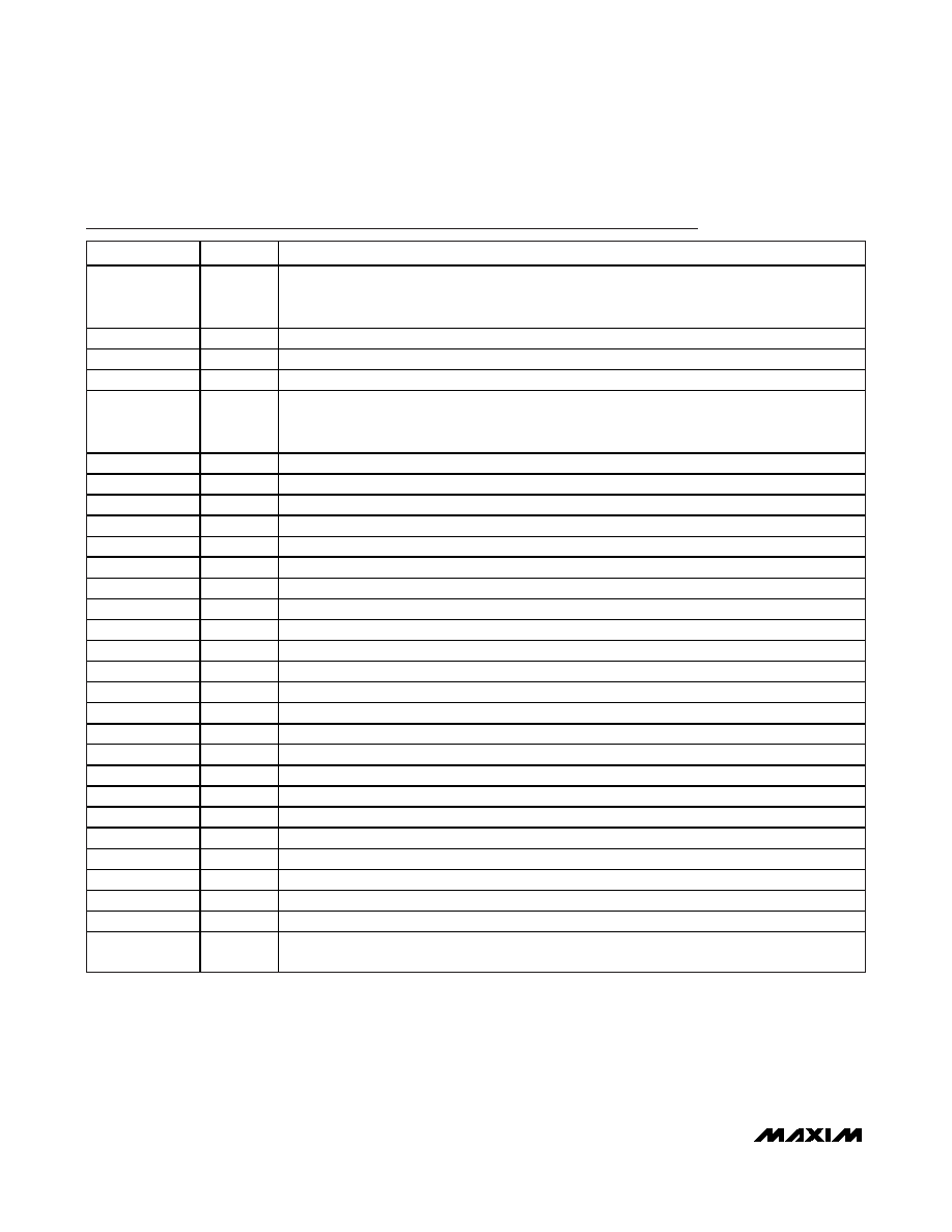
Pin Description
PIN
NAME
FUNCTION
1, 9, 16, 25, 32
VCC
Positive Supply Voltage. Bypass from VCC to VEE with 0.1F and 0.01F ceramic capacitors.
Place the capacitors as close to the device as possible with the smaller value capacitor closest to
the device.
2
N.C.
No Connection. Internally not connected.
3
CLKA
Noninverting Differential Clock Input A
4
CLKA
Inverting Differential Clock Input A
5VBB
Reference Output Voltage. Connect to the inverting or noninverting clock input to provide a
reference for single-ended operation. When used, bypass to VCC with a 0.01F ceramic
capacitor.
6
CLKB
Noninverting Differential Clock Input B
7
CLKB
Inverting Differential Clock Input B
8VEE
Negative Supply Voltage
10
QB4
Inverting QB4 Output. Typically terminate with 50
resistor to VCC - 2V.
11
QB4
Noninverting QB4 Output. Typically terminate with 50
resistor to VCC - 2V.
12
QB3
Inverting QB3 Output. Typically terminate with 50
resistor to VCC - 2V.
13
QB3
Noninverting QB3 Output. Typically terminate with 50
resistor to VCC - 2V.
14
QB2
Inverting QB2 Output. Typically terminate with 50
resistor to VCC - 2V.
15
QB2
Noninverting QB2 Output. Typically terminate with 50
resistor to VCC - 2V.
17
QB1
Inverting QB1 Output. Typically terminate with 50
resistor to VCC - 2V.
18
QB1
Noninverting QB1 Output. Typically terminate with 50
resistor to VCC - 2V.
19
QB0
Inverting QB0 Output. Typically terminate with 50
resistor to VCC - 2V.
20
QB0
Noninverting QB0 Output. Typically terminate with 50
resistor to VCC - 2V.
21
QA4
Inverting QA4 Output. Typically terminate with 50
resistor to VCC - 2V.
22
QA4
Noninverting QA4 Output. Typically terminate with 50
resistor to VCC - 2V.
23
QA3
Inverting QA3 Output. Typically terminate with 50
resistor to VCC - 2V.
24
QA3
Noninverting QA3 Output. Typically terminate with 50
resistor to VCC - 2V.
26
QA2
Inverting QA2 Output. Typically terminate with 50
resistor to VCC - 2V.
27
QA2
Noninverting QA2 Output. Typically terminate with 50
resistor to VCC - 2V.
28
QA1
Inverting QA1 Output. Typically terminate with 50
resistor to VCC - 2V.
29
QA1
Noninverting QA1 Output. Typically terminate with 50
resistor to VCC - 2V.
30
QA0
Inverting QA0 Output. Typically terminate with 50
resistor to VCC - 2V.
31
QA0
Noninverting QA0 Output. Typically terminate with 50
resistor to VCC - 2V.
—EP
Exposed Pad (TQFN package only). Internally connected to VEE. Connect EP to the VEE pad on
the PCB.
相关PDF资料 |
PDF描述 |
|---|---|
| V300A15H500BG3 | CONVERTER MOD DC/DC 15V 500W |
| V300A15H500BG2 | CONVERTER MOD DC/DC 15V 500W |
| VE-J5Z-MX | CONVERTER MOD DC/DC 2V 30W |
| AD7305BR-REEL | IC DAC 8BIT QUAD R-R 20-SOIC |
| V300A15H500BF3 | CONVERTER MOD DC/DC 15V 500W |
相关代理商/技术参数 |
参数描述 |
|---|---|
| MAX9313ECJ+T | 制造商:Maxim Integrated Products 功能描述:1:10 DIFFERENTIAL PECL/ECL/LVPECL/LVECL CLOCK AND DATA DRIVE - Tape and Reel |
| MAX9313EHJ | 制造商:Rochester Electronics LLC 功能描述: 制造商:Maxim Integrated Products 功能描述: |
| MAX9314ECJ | 制造商:Rochester Electronics LLC 功能描述: 制造商:Maxim Integrated Products 功能描述: |
| MAX9314EHJ | 制造商:Rochester Electronics LLC 功能描述: 制造商:Maxim Integrated Products 功能描述: |
| MAX9315EUP | 功能描述:时钟驱动器及分配 RoHS:否 制造商:Micrel 乘法/除法因子:1:4 输出类型:Differential 最大输出频率:4.2 GHz 电源电压-最大: 电源电压-最小:5 V 最大工作温度:+ 85 C 封装 / 箱体:SOIC-8 封装:Reel |
发布紧急采购,3分钟左右您将得到回复。