- 您现在的位置:买卖IC网 > PDF目录26790 > MAX9314EGJ (MAXIM INTEGRATED PRODUCTS INC) LOW SKEW CLOCK DRIVER, 5 TRUE OUTPUT(S), 0 INVERTED OUTPUT(S), CQCC32 PDF资料下载
参数资料
| 型号: | MAX9314EGJ |
| 厂商: | MAXIM INTEGRATED PRODUCTS INC |
| 元件分类: | 时钟及定时 |
| 英文描述: | LOW SKEW CLOCK DRIVER, 5 TRUE OUTPUT(S), 0 INVERTED OUTPUT(S), CQCC32 |
| 封装: | 5 X 5 MM, 0.90 MM HEIGHT, QFN-32 |
| 文件页数: | 6/11页 |
| 文件大小: | 337K |
| 代理商: | MAX9314EGJ |
MAX9312/MAX9314
Dual 1:5 Differential LVPECL/LVECL/HSTL
Clock and Data Drivers
4
_______________________________________________________________________________________
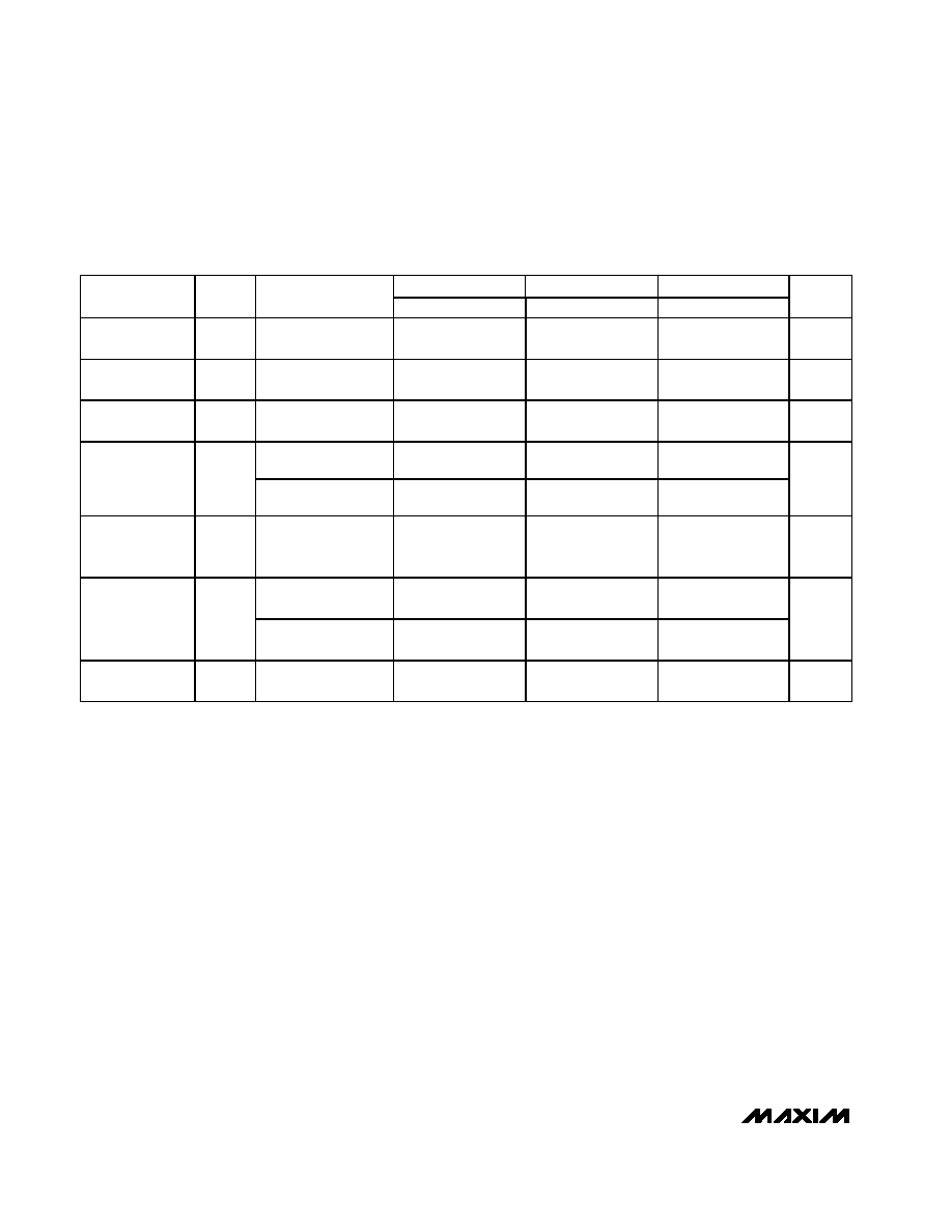
AC ELECTRICAL CHARACTERISTICS
(VCC - VEE = +2.25V to +3.8V, outputs loaded with 50
±1% to VCC - 2V, input frequency = 1.5GHz, input transition time = 125ps
(20% to 80%), VIHD = VEE + 1.2V to VCC, VILD = VEE to VCC - 0.15V, VIHD - VILD = 0.15V to the smaller of 3V or VCC - VEE, unless oth-
erwise noted. Typical values are at VCC - VEE = 3.3V, VIHD = VCC - 1V, VILD = VCC - 1.5V.) (Note 7)
-40
°C
+25
°C
+85
°C
PARAMETER
SYMBOL
CONDITIONS
MIN
TYP
MAX
MIN
TYP
MAX
MIN
TYP
MAX
UNITS
Differential Input-
to-Output Delay
tPLHD,
tPHLD
Figure 2
220
321
380
220
312
410
260
322
400
ps
Output-to-Output
Skew (Note 8)
tSKOO
12
46
12
46
10
35
ps
Part-to-Part Skew
(Note 9)
tSKPP
30
160
30
190
30
140
ps
fIN = 1.5GHz
clock pattern
1.2
2.5
1.2
2.5
1.2
2.5
Added Random
Jitter (Note 10)
tRJ
fIN = 3.0GHz
clock pattern
1.2
2.6
1.2
2.6
1.2
2.6
ps
(RMS)
Added
Deterministic
Jitter (Note 10)
tDJ
3Gbps,
223 -1 PRBS pattern
80
95
80
95
80
95
ps
(pk-pk)
VOH - VOL
≥ 300mV,
clock pattern, Figure 2
3.0
Switching
Frequency
fMAX
VOH - VOL
≥ 500mV,
clock pattern, Figure 2
1.5
GHz
Output Rise/Fall
Time (20% to 80%)
tR, tF
Figure 2
100
112
140
100
116
140
100
121
140
ps
Note 1: Measurements are made with the device in thermal equilibrium.
Note 2: Current into a pin is defined as positive. Current out of a pin is defined as negative.
Note 3: Single-ended input operation using VBB is limited to VCC - VEE = 3.0V to 3.8V for the MAX9312 and VCC - VEE = 2.7V to
3.8V for the MAX9314.
Note 4: DC parameters production tested at TA = +25°C. Guaranteed by design and characterization over the full operating temper-
ature range.
Note 5: Use VBB only for inputs that are on the same device as the VBB reference.
Note 6: All pins open except VCC and VEE.
Note 7: Guaranteed by design and characterization limits are set at ±6 sigma.
Note 8: Measured between outputs on the same part at the signal crossing points for a same-edge transition.
Note 9: Measured between outputs of different parts at the signal crossing points under identical conditions for a same-edge transition.
Note 10: Device jitter added to the input signal.
相关PDF资料 |
PDF描述 |
|---|---|
| MAX9314ECJ+ | LOW SKEW CLOCK DRIVER, 5 TRUE OUTPUT(S), 0 INVERTED OUTPUT(S), PQFP32 |
| MAX9320AEKA+ | LOW SKEW CLOCK DRIVER, 2 TRUE OUTPUT(S), 0 INVERTED OUTPUT(S), PDSO8 |
| MAX9320XESA | 9320 SERIES, LOW SKEW CLOCK DRIVER, 2 TRUE OUTPUT(S), 0 INVERTED OUTPUT(S), PDSO8 |
| MAX9325EGI | 9325 SERIES, LOW SKEW CLOCK DRIVER, 8 TRUE OUTPUT(S), 0 INVERTED OUTPUT(S), QCC28 |
| MAX9325ETI | LOW SKEW CLOCK DRIVER, 8 TRUE OUTPUT(S), 0 INVERTED OUTPUT(S), QCC28 |
相关代理商/技术参数 |
参数描述 |
|---|---|
| MAX9314EHJ | 制造商:Rochester Electronics LLC 功能描述: 制造商:Maxim Integrated Products 功能描述: |
| MAX9315EUP | 功能描述:时钟驱动器及分配 RoHS:否 制造商:Micrel 乘法/除法因子:1:4 输出类型:Differential 最大输出频率:4.2 GHz 电源电压-最大: 电源电压-最小:5 V 最大工作温度:+ 85 C 封装 / 箱体:SOIC-8 封装:Reel |
| MAX9315EUP+ | 功能描述:时钟驱动器及分配 LVPECL/LVECL/HSTL Clock & Data Driver RoHS:否 制造商:Micrel 乘法/除法因子:1:4 输出类型:Differential 最大输出频率:4.2 GHz 电源电压-最大: 电源电压-最小:5 V 最大工作温度:+ 85 C 封装 / 箱体:SOIC-8 封装:Reel |
| MAX9315EUP+T | 功能描述:时钟驱动器及分配 LVPECL/LVECL/HSTL Clock & Data Driver RoHS:否 制造商:Micrel 乘法/除法因子:1:4 输出类型:Differential 最大输出频率:4.2 GHz 电源电压-最大: 电源电压-最小:5 V 最大工作温度:+ 85 C 封装 / 箱体:SOIC-8 封装:Reel |
| MAX9315EUP-T | 功能描述:时钟驱动器及分配 RoHS:否 制造商:Micrel 乘法/除法因子:1:4 输出类型:Differential 最大输出频率:4.2 GHz 电源电压-最大: 电源电压-最小:5 V 最大工作温度:+ 85 C 封装 / 箱体:SOIC-8 封装:Reel |
发布紧急采购,3分钟左右您将得到回复。