- 您现在的位置:买卖IC网 > PDF目录8679 > MAX9321EKA+T (Maxim Integrated Products)IC CLOCK/DATA DRVR 1:1 8SOIC PDF资料下载
参数资料
| 型号: | MAX9321EKA+T |
| 厂商: | Maxim Integrated Products |
| 文件页数: | 2/9页 |
| 文件大小: | 0K |
| 描述: | IC CLOCK/DATA DRVR 1:1 8SOIC |
| 标准包装: | 2,500 |
| 类型: | 时钟/数据驱动器 |
| 电路数: | 1 |
| 比率 - 输入:输出: | 1:1 |
| 差分 - 输入:输出: | 是/是 |
| 输入: | HSTL,LVECL,LVPECL |
| 输出: | LVECL,LVPECL |
| 频率 - 最大: | 3GHz |
| 电源电压: | 2.25 V ~ 3.8 V |
| 工作温度: | -40°C ~ 85°C |
| 安装类型: | * |
| 封装/外壳: | * |
| 供应商设备封装: | * |
| 包装: | * |
MAX9321/MAX9321A
Differential LVPECL/LVECL/HSTL
Receiver/Drivers
2
_______________________________________________________________________________________
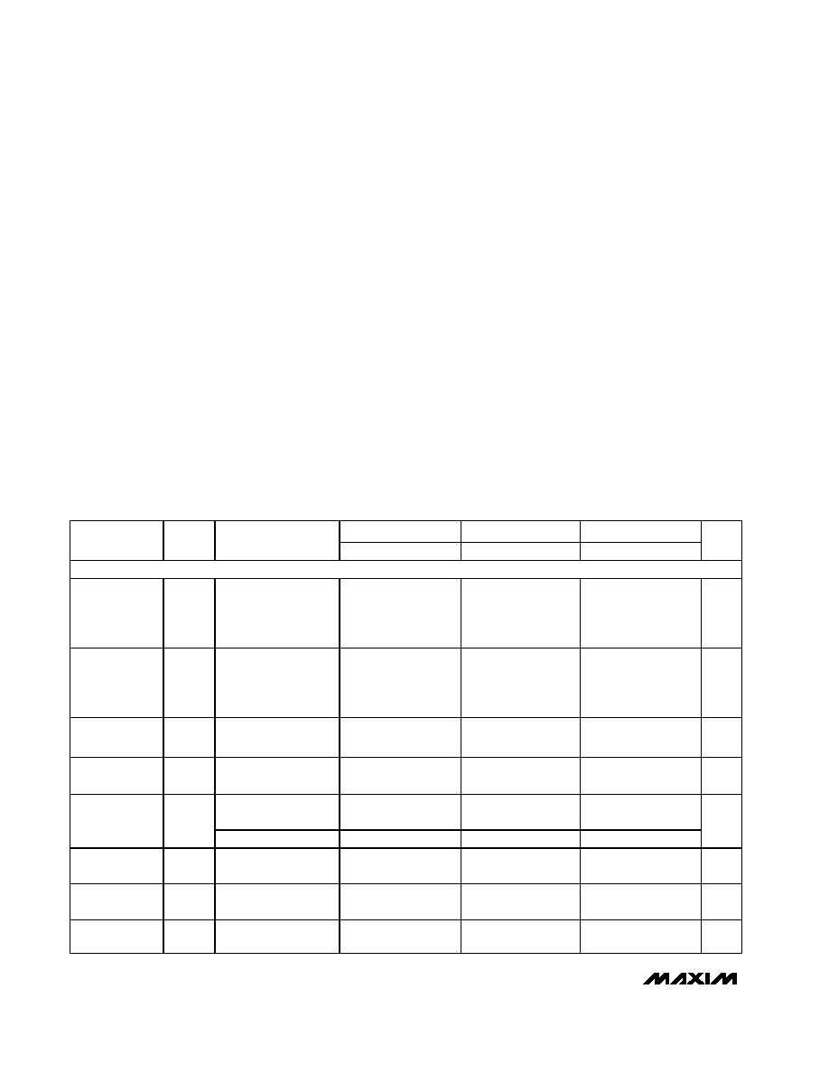
ABSOLUTE MAXIMUM RATINGS
DC ELECTRICAL CHARACTERISTICS
(VCC - VEE = +2.25V to +3.8V, outputs loaded with 50
±1% to VCC - 2.0V. Typical values are at VCC - VEE = +3.3V, VIHD = VCC - 1V,
VILD = VCC - 1.5V, unless otherwise noted.) (Notes 1–5)
Stresses beyond those listed under “Absolute Maximum Ratings” may cause permanent damage to the device. These are stress ratings only, and functional
operation of the device at these or any other conditions beyond those indicated in the operational sections of the specifications is not implied. Exposure to
absolute maximum rating conditions for extended periods may affect device reliability.
VCC to VEE ..........................................................................+4.1V
D or D .................................................. VEE - 0.3V to VCC + 0.3V
D to D .................................................................................±3.0V
Continuous Output Current .................................................50mA
Surge Output Current........................................................100mA
VBB Sink/Source Current .................................................±0.6mA
Junction-to-Ambient Thermal Resistance in Still Air
8-Pin SOT23.............................................................+112°C/W
8-Pin MAX ..............................................................+221°C/W
8-Pin SO-EP ...............................................................+53°C/W
Junction-to-Ambient Thermal Resistance with
500 LFPM Airflow
8-Pin SOT23...............................................................+78°C/W
8-Pin MAX ..............................................................+155°C/W
8-Pin SO.....................................................................+99°C/W
Junction-to-Case Thermal Resistance
8-Pin SOT23...............................................................+80°C/W
8-Pin MAX ................................................................+39°C/W
8-Pin SO.....................................................................+40°C/W
Operating Temperature Range ...........................-40°C to +85°C
Junction Temperature ......................................................+150°C
Storage Temperature Range .............................-65°C to +150°C
ESD Protection
Human Body Model (D, D, Q, Q, VBB).............................>2kV
Soldering Temperature (10s) ...........................................+300°C
-40
°C
+25
°C
+85
°C
PARAMETER
SYMBOL
CONDITIONS
MIN
TYP
MAX
MIN
TYP
MAX
MIN
TYP
MAX
UNITS
DIFFERENTIAL INPUT (D, D)
Single-Ended
Input High
Voltage
VIH
VBB connected to D
(VIL for VBB
connected to D),
Figure 1
VCC -
1.210
VCC
VCC -
1.145
VCC
VCC -
1.085
VCC
V
Single-Ended
Input Low
Voltage
VIL
VBB connected to D
(VIH for VBB
connected to D),
Figure 1
VEE
VCC -
1.65
VEE
VCC -
1.545
VEE
VCC -
1.485
V
High Voltage of
Differential
Input
VIHD
VEE +
1.2
VCC
VEE +
1.2
VCC
VEE +
1.2
VCC
V
Low Voltage of
Differential
Input
VILD
VEE
VCC -
0.1
VEE
VCC -
0.1
VEE
VCC -
0.1
V
For VCC - VEE
< 3.0V
0.1
VCC -
VEE
0.1
VCC -
VEE
0.1
VCC -
VEE
Differential
Input Voltage
VIHD -
VILD
For VCC - VEE
≥ 3.0V
0.1
3.0
0.1
3.0
0.1
3.0
V
Input High
Current
IIH
150
A
D Input Low
Current
IILD
-10
100
-10
100
-10
100
A
D Input Low
Current
IILD
-150
+150
-150
+150
-150
+150
A
相关PDF资料 |
PDF描述 |
|---|---|
| V300A15H500B3 | CONVERTER MOD DC/DC 15V 500W |
| MAX9321EUA+ | IC CLOCK/DATA DRIVER 1:1 8-UMAX |
| V300A15H500B2 | CONVERTER MOD DC/DC 15V 500W |
| MAX9320EUA+ | IC CLOCK BUFFER 2:2 3GHZ 8-UMAX |
| DAC8512FSZ-REEL7 | IC DAC 12BIT SRL LP 5V 8SOIC |
相关代理商/技术参数 |
参数描述 |
|---|---|
| MAX9321ESA | 制造商:Maxim Integrated Products 功能描述:DIFFERENTIAL LVPECL/LVECL/HSTL RECEIVER/DRIVE - Rail/Tube 制造商:Rochester Electronics LLC 功能描述: |
| MAX9321EUA | 制造商:Maxim Integrated Products 功能描述:DIFFERENTIAL LVPECL/LVECL/HSTL RECEIVER/DRIVE - Rail/Tube |
| MAX9321EUA+ | 功能描述:总线收发器 LVPECL/LVECL/HSTL Receiver/Driver RoHS:否 制造商:Fairchild Semiconductor 逻辑类型:CMOS 逻辑系列:74VCX 每芯片的通道数量:16 输入电平:CMOS 输出电平:CMOS 输出类型:3-State 高电平输出电流:- 24 mA 低电平输出电流:24 mA 传播延迟时间:6.2 ns 电源电压-最大:2.7 V, 3.6 V 电源电压-最小:1.65 V, 2.3 V 最大工作温度:+ 85 C 封装 / 箱体:TSSOP-48 封装:Reel |
| MAX9321EUA+T | 功能描述:时钟驱动器及分配 LVPECL/LVECL/HSTL Receiver/Driver RoHS:否 制造商:Micrel 乘法/除法因子:1:4 输出类型:Differential 最大输出频率:4.2 GHz 电源电压-最大: 电源电压-最小:5 V 最大工作温度:+ 85 C 封装 / 箱体:SOIC-8 封装:Reel |
| MAX9322ECY+ | 制造商:Maxim Integrated Products 功能描述:DIFFERENTIAL DIVIDE-BY-1/DIVIDE-BY-2 CLOCK DRVR 52TQFP - Rail/Tube |
发布紧急采购,3分钟左右您将得到回复。