- 您现在的位置:买卖IC网 > PDF目录10339 > MAX9775EBX+TG45 (Maxim Integrated Products)IC AMP AUDIO PWR 1.5W STER 36WLP PDF资料下载
参数资料
| 型号: | MAX9775EBX+TG45 |
| 厂商: | Maxim Integrated Products |
| 文件页数: | 18/38页 |
| 文件大小: | 0K |
| 描述: | IC AMP AUDIO PWR 1.5W STER 36WLP |
| 产品培训模块: | Lead (SnPb) Finish for COTS Obsolescence Mitigation Program |
| 标准包装: | 2,500 |
| 系列: | DirectDrive® |
| 类型: | D 类 |
| 输出类型: | 2-通道(立体声)带立体声耳机 |
| 在某负载时最大输出功率 x 通道数量: | 1.5W x 2 @ 4 欧姆; 60mW x 2 @ 16 欧姆 |
| 电源电压: | 2.7 V ~ 5.5 V |
| 特点: | 3D,消除爆音,差分输入,I²C,静音,短路和热保护,关机,音量控制 |
| 安装类型: | 表面贴装 |
| 供应商设备封装: | 36-WLP |
| 封装/外壳: | 36-UFBGA,WLCSP |
| 包装: | 带卷 (TR) |
第1页第2页第3页第4页第5页第6页第7页第8页第9页第10页第11页第12页第13页第14页第15页第16页第17页当前第18页第19页第20页第21页第22页第23页第24页第25页第26页第27页第28页第29页第30页第31页第32页第33页第34页第35页第36页第37页第38页
Click-and-Pop Suppression
In conventional single-supply headphone amplifiers, the
output-coupling capacitor is a major contributor of audi-
ble clicks and pops. Upon startup, the amplifier charges
the coupling capacitor to its bias voltage, typically half the
supply. Likewise, during shutdown, the capacitor is dis-
charged to GND. This results in a DC shift across the
capacitor, which, in turn, appears as an audible transient
at the speaker. Since the MAX9775/MAX9776 headphone
amplifier does not require output-coupling capacitors, this
problem does not arise.
In most applications, the output of the preamplifier dri-
ving the MAX9775/MAX9776 has a DC bias of typically
half the supply. During startup, the input-coupling
capacitor is charged to the preamplifier’s DC bias volt-
age, resulting in a DC shift across the capacitor and an
audible click/pop. An internal delay of 30ms eliminates
the click/pop caused by the input filter.
Shutdown
The MAX9775/MAX9776 feature a 0.1A hard shutdown
mode that reduces power consumption to extend battery
life and a soft shutdown where current consumption is
typically 8.5A. Hard shutdown is controlled by connect-
ing the SHDN pin to GND, disabling the amplifiers, bias
circuitry, charge pump, and I2C. In shutdown, the head-
phone amplifier output impedance is 1.4k
Ω and the
speaker output impedance is 300k
Ω. Similarly, the
MAX9775/MAX9776 enter soft-shutdown when the SHDN
bit = 0 (see Table 2). The I2C interface is active and the
contents of the command register are not affected when
in soft-shutdown. This allows the master to write to the
MAX9775/MAX9776 while in shutdown. The I2C interface
is completely disabled in hardware shutdown. When the
MAX9775/MAX9776 are re-enabled the default settings
are applied (see Table 3).
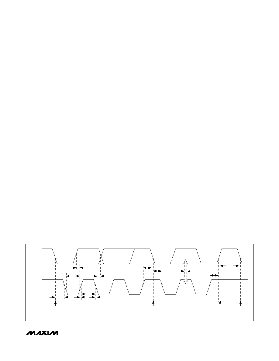
I2C Interface
The MAX9775/MAX9776 feature an I2C 2-wire serial
interface consisting of a serial data line (SDA) and a
serial clock line (SCL). SDA and SCL facilitate commu-
nication between the MAX9775/MAX9776 and the mas-
ter at clock rates up to 400kHz. Figure 8 shows the
2-wire interface timing diagram. The MAX9775/
MAX9776 are receive-only slave devices relying on the
master to generate the SCL signal. The master, typical-
ly a microcontroller, generates SCL and initiates data
transfer on the bus. The MAX9775/MAX9776 cannot
write to the SDA bus except to acknowledge the receipt
of data from the master. The MAX9775/MAX9776 will
not acknowledge a read command from the master.
A master device communicates to the MAX9775/
MAX9776 by transmitting the proper address followed
by the data word. Each transmit sequence is framed by
a START (S) or REPEATED START (Sr) condition and a
STOP (P) condition. Each word transmitted over the
bus is 8 bits long and is always followed by an
acknowledge clock pulse.
The MAX9775/MAX9776 SDA line operates as both an
input and an open-drain output. A pullup resistor,
greater than 500
Ω, is required on the SDA bus. The
MAX9775/MAX9776 SCL line operates as an input only.
A pullup resistor (greater than 500
Ω) is required on
SCL if there are multiple masters on the bus or if the
master in a single-master system has an open-drain
SCL output. Series resistors in line with SDA and SCL
are optional. Series resistors protect the digital inputs of
the MAX9775/MAX9776 from high-voltage spikes on
the bus lines, and minimize crosstalk and undershoot of
the bus signals.
MAX9775/MAX9776
2 x 1.5W, Stereo Class D Audio Subsystem
with DirectDrive Headphone Amplifier
______________________________________________________________________________________
25
SCL
SDA
START
CONDITION
STOP
CONDITION
REPEATED
START
CONDITION
START
CONDITION
tHD, STA
tSU, STA
tHD, STA
tSP
tBUF
tSU, STO
tLOW
tSU, DAT
tHD, DAT
tHIGH
tR
tF
Figure 8. 2-Wire Serial-Interface Timing Diagram
相关PDF资料 |
PDF描述 |
|---|---|
| AD7277ARMZ | IC ADC 10BIT SER 3MSPS 8MSOP |
| MS27499E12A35PA | CONN RCPT 22POS BOX MNT W/PINS |
| VE-J6D-IW-B1 | CONVERTER MOD DC/DC 85V 100W |
| MAX98400BETG+T | IC AMP AUDIO STEREO D 24TQFN |
| D38999/26FD19PALC | CONN HSG PLUG 19POS STRGHT PINS |
相关代理商/技术参数 |
参数描述 |
|---|---|
| MAX9776EBX+TG45 | 功能描述:音频放大器 2 x 1.5W Stereo Class D Subsystem RoHS:否 制造商:STMicroelectronics 产品:General Purpose Audio Amplifiers 输出类型:Digital 输出功率: THD + 噪声: 工作电源电压:3.3 V 电源电流: 最大功率耗散: 最大工作温度: 安装风格:SMD/SMT 封装 / 箱体:TQFP-64 封装:Reel |
| MAX9776ETJ+ | 功能描述:音频放大器 2 x 1.5W Stereo Class D Subsystem RoHS:否 制造商:STMicroelectronics 产品:General Purpose Audio Amplifiers 输出类型:Digital 输出功率: THD + 噪声: 工作电源电压:3.3 V 电源电流: 最大功率耗散: 最大工作温度: 安装风格:SMD/SMT 封装 / 箱体:TQFP-64 封装:Reel |
| MAX9776ETJ+T | 功能描述:音频放大器 2 x 1.5W Stereo Class D Subsystem RoHS:否 制造商:STMicroelectronics 产品:General Purpose Audio Amplifiers 输出类型:Digital 输出功率: THD + 噪声: 工作电源电压:3.3 V 电源电流: 最大功率耗散: 最大工作温度: 安装风格:SMD/SMT 封装 / 箱体:TQFP-64 封装:Reel |
| MAX9776EVKIT+ | 功能描述:音频 IC 开发工具 MAX9776 Eval Kit RoHS:否 制造商:Texas Instruments 产品:Evaluation Kits 类型:Audio Amplifiers 工具用于评估:TAS5614L 工作电源电压:12 V to 38 V |
| MAX9777ETI+ | 功能描述:音频放大器 Integrated Circuits (ICs) RoHS:否 制造商:STMicroelectronics 产品:General Purpose Audio Amplifiers 输出类型:Digital 输出功率: THD + 噪声: 工作电源电压:3.3 V 电源电流: 最大功率耗散: 最大工作温度: 安装风格:SMD/SMT 封装 / 箱体:TQFP-64 封装:Reel |
发布紧急采购,3分钟左右您将得到回复。