- 您现在的位置:买卖IC网 > PDF目录10340 > MAX9789BETJ+T (Maxim Integrated Products)IC AMP AUDIO 2W STER AB 32TQFN PDF资料下载
参数资料
| 型号: | MAX9789BETJ+T |
| 厂商: | Maxim Integrated Products |
| 文件页数: | 10/28页 |
| 文件大小: | 0K |
| 描述: | IC AMP AUDIO 2W STER AB 32TQFN |
| 产品培训模块: | Lead (SnPb) Finish for COTS Obsolescence Mitigation Program |
| 标准包装: | 2,500 |
| 系列: | DirectDrive® |
| 类型: | AB 类 |
| 输出类型: | 2-通道(立体声)带立体声耳机 |
| 在某负载时最大输出功率 x 通道数量: | 2W x 2 @ 4 欧姆; 100mW x 2 @ 16 欧姆 |
| 电源电压: | 4.5 V ~ 5.5 V |
| 特点: | 消除爆音,静音,短路保护和热保护,关机 |
| 安装类型: | 表面贴装 |
| 供应商设备封装: | 32-TQFN-EP(5x5) |
| 封装/外壳: | 32-WFQFN 裸露焊盘 |
| 包装: | 带卷 (TR) |
第1页第2页第3页第4页第5页第6页第7页第8页第9页当前第10页第11页第12页第13页第14页第15页第16页第17页第18页第19页第20页第21页第22页第23页第24页第25页第26页第27页第28页
MAX9789/MAX9790
Windows Vista-Compliant, Stereo Class AB Speaker
Amplifiers and DirectDrive Headphone Amplifiers
18
______________________________________________________________________________________
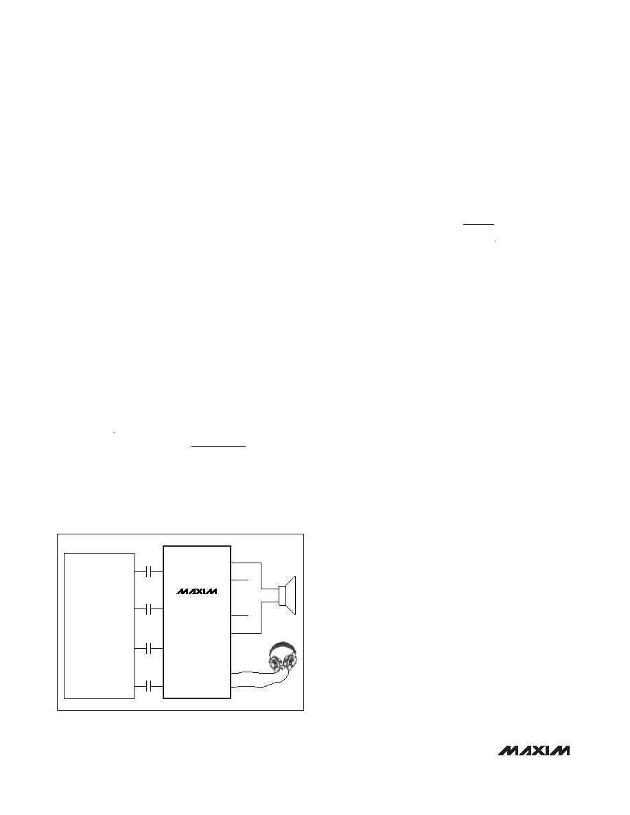
Mono Speaker Configuration
The MAX9789 stereo BTL Class AB speaker amplifier
can be configured to drive a mono speaker. Rather
than combining the CODEC’s left- and right-input sig-
nals in a resistive network prior to one channel of the
speaker amplifier input, the transducer itself can be
connected to the BTL speaker amplifier output as
shown in Figure 6. When compared to the resistive net-
work implementation, the configuration in Figure 6 will:
1) Eliminate noise pickup by eliminating the high-
impedance node at the CODEC’s left- and right-
signal mixing point. SNR performance will be
improved as a result.
2) Eliminate gain error by eliminating any resistive
mismatch between the external resistance used to
sum the left and right signals and the MAX9789
internal resistance.
Power Dissipation and Heat Sinking
Under normal operating conditions, the MAX9789/
MAX9790 can dissipate a significant amount of power.
The maximum power dissipation for each package is
given in the
Absolute Maximum Ratings section under
Continuous Power Dissipation, or can be calculated by
the following equation:
where TJ(MAX) is +150°C, TA is the ambient tempera-
ture, and
θJA is the reciprocal of the derating factor in
°C/W as specified in the
Absolute Maximum Ratings
section. For example,
θJA for the 32-pin TQFN-EP pack-
age is +40.2°C/W for a multilayer PC board.
Output Power (Speaker Amplifier)
The increase in power delivered by the BTL configura-
tion directly results in an increase in internal power dis-
sipation over the single-ended configuration. The
maximum power dissipation for a given VDD and load is
given by the following equation:
If the power dissipation for a given application exceeds
the maximum allowed for a given package, either reduce
VDD, increase load impedance, decrease the ambient
temperature, or add heat sinking to the device. Large
output, supply, and ground PC board traces improve the
maximum power dissipation in the package.
Thermal-overload protection limits total power dissipa-
tion in these devices. When the junction temperature
exceeds +150°C, the thermal-protection circuitry dis-
ables the amplifier output stage. The amplifiers are
enabled once the junction temperature cools by +15°C.
This results in a pulsing output under continuous ther-
mal-overload conditions as the device heats and cools.
Power Supplies
The MAX9789/MAX9790 have separate supply pins for
each portion of the device, allowing for the optimum
combination of headroom and power dissipation and
noise immunity. The speaker amplifiers are powered
from PVDD. PVDD ranges from 4.5V to 5.5V. The head-
phone amplifiers are powered from HPVDD and PVSS.
HPVDD is the positive supply of the headphone ampli-
fiers and ranges from 3V to 5.5V. PVSS is the negative
supply of the headphone amplifiers. Connect PVSS to
CPVSS. The charge pump is powered by CPVDD.
CPVDD ranges from 3V to 5.5V and should be the same
potential as HPVDD. The charge pump inverts the volt-
age at CPVDD, and the resulting voltage appears at
CPVSS. The internal LDO and the remainder of the
device is powered by VDD.
Component Selection
Supply Bypassing
The MAX9789/MAX9790 have separate supply pins for
each portion of the device, allowing for the optimum
combination of headroom and power dissipation and
noise immunity.
Speaker Amplifier Power-Supply Input (PVDD)
The speaker amplifiers are powered from PVDD. PVDD
ranges from 4.5V to 5.5V. Bypass PVDD with a 0.1F
capacitor to PGND. Note additional bulk capacitance is
required at the device if long input traces between
PVDD and the power source are used.
P
V
R
DISS MAX
DD
L
() =
2
π
P
TT
DISSPKG MAX
J MAX
A
JA
()
=
θ
SPKR_OUTL
SPKR_OUTR
SPKR_INL
SPKR_INR
OUTL+
OUTL-
OUTR+
OUTR-
CODEC
CIN1
LINE_OUTR
LINE_OUTL
HP_INL
HP_INR
HPL
HPR
MAX9789
CIN1
CIN2
Figure 6. Mono Signal Output Configuration for MAX9789
相关PDF资料 |
PDF描述 |
|---|---|
| MS27508E10F13PB | CONN RCPT 13POS BOX MNT W/PINS |
| TA3MX | CONN PLUG CORD 3POS MALE MINI |
| MS27467E15B19PA | CONN PLUG 19POS STRAIGHT W/PINS |
| AAA7MBZ | CONN PLUG MALE 7PIN SILVER BLK |
| MAX9792CETI+T | IC AMP AUDIO 2.0W STER D 28TQFN |
相关代理商/技术参数 |
参数描述 |
|---|---|
| MAX9789CETJ+ | 功能描述:音频放大器 Windows Vista Class AB Speaker Amp RoHS:否 制造商:STMicroelectronics 产品:General Purpose Audio Amplifiers 输出类型:Digital 输出功率: THD + 噪声: 工作电源电压:3.3 V 电源电流: 最大功率耗散: 最大工作温度: 安装风格:SMD/SMT 封装 / 箱体:TQFP-64 封装:Reel |
| MAX9789CETJ+T | 功能描述:音频放大器 Windows Vista Class AB Speaker Amp RoHS:否 制造商:STMicroelectronics 产品:General Purpose Audio Amplifiers 输出类型:Digital 输出功率: THD + 噪声: 工作电源电压:3.3 V 电源电流: 最大功率耗散: 最大工作温度: 安装风格:SMD/SMT 封装 / 箱体:TQFP-64 封装:Reel |
| MAX978EEE | 功能描述:校验器 IC Quad High Speed Comparator RoHS:否 制造商:STMicroelectronics 产品: 比较器类型: 通道数量: 输出类型:Push-Pull 电源电压-最大:5.5 V 电源电压-最小:1.1 V 补偿电压(最大值):6 mV 电源电流(最大值):1350 nA 响应时间: 最大工作温度:+ 125 C 安装风格:SMD/SMT 封装 / 箱体:SC-70-5 封装:Reel |
| MAX978EEE+ | 功能描述:校验器 IC Quad High Speed Comparator RoHS:否 制造商:STMicroelectronics 产品: 比较器类型: 通道数量: 输出类型:Push-Pull 电源电压-最大:5.5 V 电源电压-最小:1.1 V 补偿电压(最大值):6 mV 电源电流(最大值):1350 nA 响应时间: 最大工作温度:+ 125 C 安装风格:SMD/SMT 封装 / 箱体:SC-70-5 封装:Reel |
| MAX978EEE+T | 功能描述:校验器 IC Quad High Speed Comparator RoHS:否 制造商:STMicroelectronics 产品: 比较器类型: 通道数量: 输出类型:Push-Pull 电源电压-最大:5.5 V 电源电压-最小:1.1 V 补偿电压(最大值):6 mV 电源电流(最大值):1350 nA 响应时间: 最大工作温度:+ 125 C 安装风格:SMD/SMT 封装 / 箱体:SC-70-5 封装:Reel |
发布紧急采购,3分钟左右您将得到回复。