- 您现在的位置:买卖IC网 > PDF目录10340 > MAX9789BETJ+T (Maxim Integrated Products)IC AMP AUDIO 2W STER AB 32TQFN PDF资料下载
参数资料
| 型号: | MAX9789BETJ+T |
| 厂商: | Maxim Integrated Products |
| 文件页数: | 12/28页 |
| 文件大小: | 0K |
| 描述: | IC AMP AUDIO 2W STER AB 32TQFN |
| 产品培训模块: | Lead (SnPb) Finish for COTS Obsolescence Mitigation Program |
| 标准包装: | 2,500 |
| 系列: | DirectDrive® |
| 类型: | AB 类 |
| 输出类型: | 2-通道(立体声)带立体声耳机 |
| 在某负载时最大输出功率 x 通道数量: | 2W x 2 @ 4 欧姆; 100mW x 2 @ 16 欧姆 |
| 电源电压: | 4.5 V ~ 5.5 V |
| 特点: | 消除爆音,静音,短路保护和热保护,关机 |
| 安装类型: | 表面贴装 |
| 供应商设备封装: | 32-TQFN-EP(5x5) |
| 封装/外壳: | 32-WFQFN 裸露焊盘 |
| 包装: | 带卷 (TR) |
第1页第2页第3页第4页第5页第6页第7页第8页第9页第10页第11页当前第12页第13页第14页第15页第16页第17页第18页第19页第20页第21页第22页第23页第24页第25页第26页第27页第28页
MAX9789/MAX9790
Windows Vista-Compliant, Stereo Class AB Speaker
Amplifiers and DirectDrive Headphone Amplifiers
2
_______________________________________________________________________________________
ABSOLUTE MAXIMUM RATINGS
ELECTRICAL CHARACTERISTICS
(VDD = PVDD = CPVDD = HPVDD = HP_EN = VLDO_EN (MAX9789 only) = +5V, VGND = VPGND = VCPGND = SPKR_EN = VLDO_SET
(MAX9789 only) = 0V, ILDO_OUT (MAX9789 only) = 0, C1 = C2 = CBIAS = 1F. RL = ∞, unless otherwise specified, VGAIN1 = 0,
VGAIN2 = 5V (AVSP = 10dB, AVHP = 3.5dB), TA = TMIN to TMAX, unless otherwise noted. Typical values are at TA = +25°C.) (Note 2)
Stresses beyond those listed under “Absolute Maximum Ratings” may cause permanent damage to the device. These are stress ratings only, and functional
operation of the device at these or any other conditions beyond those indicated in the operational sections of the specifications is not implied. Exposure to
absolute maximum rating conditions for extended periods may affect device reliability.
Supply Voltage (VDD, PVDD, HPVDD,
CPVDD to GND) ..................................................-0.3V to +6.0V
GND to PGND, CPGND ......................................................±0.3V
CPVSS, C1N, VSS to GND......................................-6.0V to +0.3V
HPR, HPL to GND ...............................................................±3.0V
Any Other Pin .............................................-0.3V to (VDD + 0.3V)
Duration of OUT_+, OUT_- Short Circuit
to GND or PVDD ......................................................Continuous
Duration of Short Circuit between OUT_+, OUT_-
and LDO_OUT.........................................................Continuous
Duration of Short Circuit between HPR, HPL and GND,
VSS or HPVDD..........................................................Continuous
Continuous Current (PVDD, OUT_+, OUT_-, PGND).............1.7A
Continuous Current (CPVDD, C1N, C1P, CPVSS, PVSS,
VDD, HPVDD, LDO_OUT, HPR, HPL) .............................850mA
Continuous Input Current (all other pins) .........................±20mA
Continuous Power Dissipation (TA = +70°C)
32-Pin Thin QFN Single-Layer Board
(derate 18.6mW/°C above +70°C) ..............................1489mW
θJA...........................................................................53.7°C/W
θJC...........................................................................19.9°C/W
32-Pin Thin QFN Multilayer Board
(derate 24.9 mW/°C above +70°C) .............................1990mW
θJA...........................................................................40.2°C/W
θJC...........................................................................19.9°C/W
Operating Temperature Range ...........................-40°C to +85°C
Junction Temperature ......................................................+150°C
Storage Temperature Range .............................-65°C to +150°C
Lead Temperature (soldering, 10s) .................................+300°C
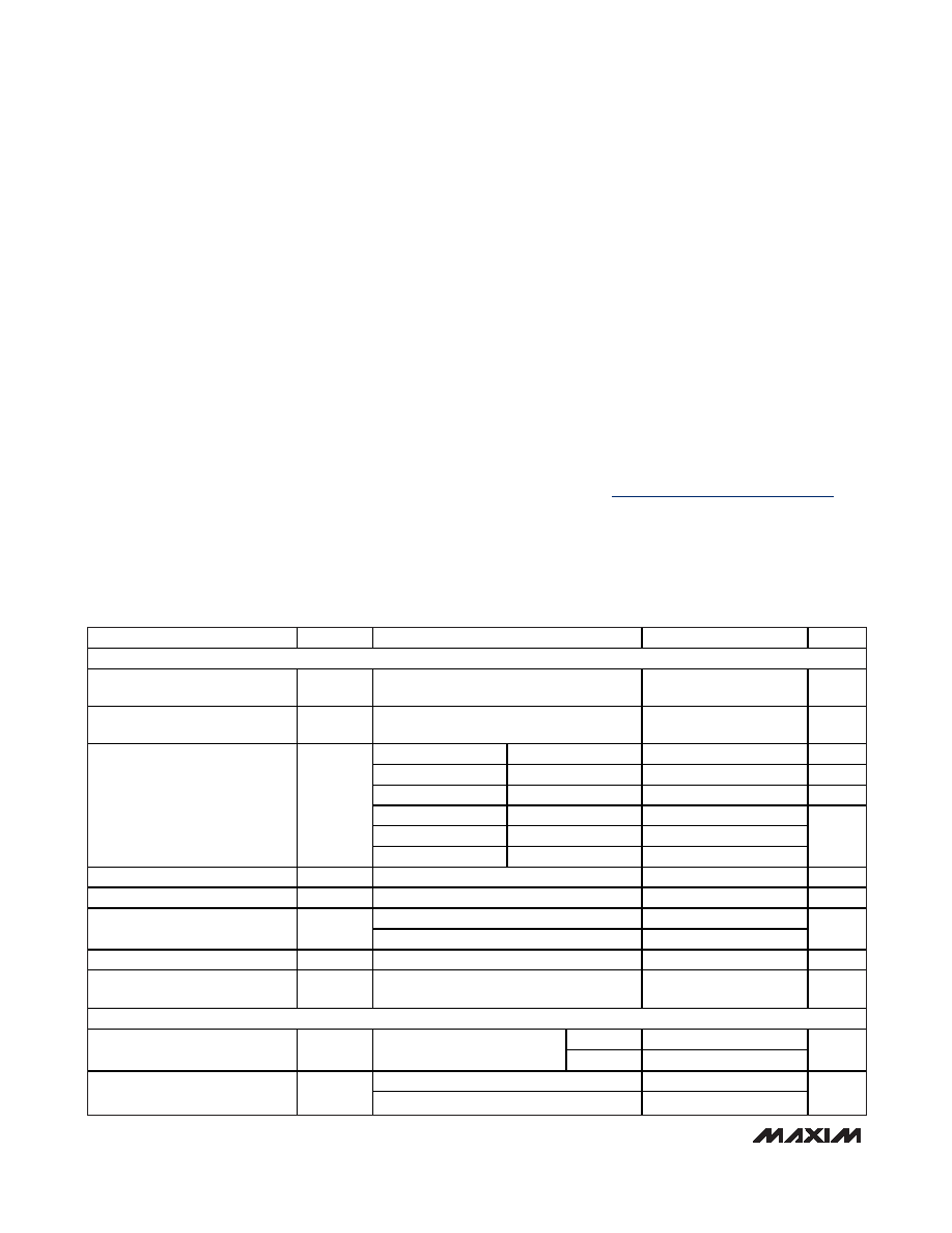
PARAMETER
SYMBOL
CONDITIONS
MIN
TYP
MAX
UNITS
GENERAL
Supply Voltage
VDD, PVDD
Guaranteed by PSRR and LDO Line
Regulation Tests
4.5
5.5
V
Headphone Supply Voltage
CPVDD,
HPVDD
Guaranteed by PSRR Test
3.0
5.5
V
SPKR_EN
HP_EN
1 (MAX9789)
0 (MAX9789)
0.1
0.4
mA
1 (MAX9790)
0 (MAX9790)
0.3
6
A
11
7
13
0
14
29
Quiescent Current
IDD
0
1
18
40
mA
Shutdown Current
ISHDN
SPKR_EN = VDD, HP_EN = LDO_EN = GND
0.3
6
A
Bias Voltage
VBIAS
1.7
1.8
1.9
V
MAX9789A/MAX9789C/MAX9790A
100
Shutdown to Full Operation
tSON
MAX9789B/MAX9790B
25
ms
Gain Switching Time
tSW
10
s
Channel-to-Channel Gain
Tracking
±0.1
dB
SPEAKER AMPLIFIER
RL = 4
Ω
2
Output Power
POUT
THD+N = 1%, f = 1kHz,
TA = +25°C
RL = 8
Ω
1
W
RL = 8
Ω, POUT = 1W, f = 1kHz
0.002
Total Harmonic Distortion Plus
Noise
THD+N
RL = 4
Ω, POUT = 1W, f = 1kHz
0.004
%
Note 1: Package thermal resistances were obtained using the method described in JEDEC specification JESD51-7 using a four-
layer board. For detailed information on package thermal considerations, refer to www.maxim-ic.com/thermal-tutorial.
相关PDF资料 |
PDF描述 |
|---|---|
| MS27508E10F13PB | CONN RCPT 13POS BOX MNT W/PINS |
| TA3MX | CONN PLUG CORD 3POS MALE MINI |
| MS27467E15B19PA | CONN PLUG 19POS STRAIGHT W/PINS |
| AAA7MBZ | CONN PLUG MALE 7PIN SILVER BLK |
| MAX9792CETI+T | IC AMP AUDIO 2.0W STER D 28TQFN |
相关代理商/技术参数 |
参数描述 |
|---|---|
| MAX9789CETJ+ | 功能描述:音频放大器 Windows Vista Class AB Speaker Amp RoHS:否 制造商:STMicroelectronics 产品:General Purpose Audio Amplifiers 输出类型:Digital 输出功率: THD + 噪声: 工作电源电压:3.3 V 电源电流: 最大功率耗散: 最大工作温度: 安装风格:SMD/SMT 封装 / 箱体:TQFP-64 封装:Reel |
| MAX9789CETJ+T | 功能描述:音频放大器 Windows Vista Class AB Speaker Amp RoHS:否 制造商:STMicroelectronics 产品:General Purpose Audio Amplifiers 输出类型:Digital 输出功率: THD + 噪声: 工作电源电压:3.3 V 电源电流: 最大功率耗散: 最大工作温度: 安装风格:SMD/SMT 封装 / 箱体:TQFP-64 封装:Reel |
| MAX978EEE | 功能描述:校验器 IC Quad High Speed Comparator RoHS:否 制造商:STMicroelectronics 产品: 比较器类型: 通道数量: 输出类型:Push-Pull 电源电压-最大:5.5 V 电源电压-最小:1.1 V 补偿电压(最大值):6 mV 电源电流(最大值):1350 nA 响应时间: 最大工作温度:+ 125 C 安装风格:SMD/SMT 封装 / 箱体:SC-70-5 封装:Reel |
| MAX978EEE+ | 功能描述:校验器 IC Quad High Speed Comparator RoHS:否 制造商:STMicroelectronics 产品: 比较器类型: 通道数量: 输出类型:Push-Pull 电源电压-最大:5.5 V 电源电压-最小:1.1 V 补偿电压(最大值):6 mV 电源电流(最大值):1350 nA 响应时间: 最大工作温度:+ 125 C 安装风格:SMD/SMT 封装 / 箱体:SC-70-5 封装:Reel |
| MAX978EEE+T | 功能描述:校验器 IC Quad High Speed Comparator RoHS:否 制造商:STMicroelectronics 产品: 比较器类型: 通道数量: 输出类型:Push-Pull 电源电压-最大:5.5 V 电源电压-最小:1.1 V 补偿电压(最大值):6 mV 电源电流(最大值):1350 nA 响应时间: 最大工作温度:+ 125 C 安装风格:SMD/SMT 封装 / 箱体:SC-70-5 封装:Reel |
发布紧急采购,3分钟左右您将得到回复。