- 您现在的位置:买卖IC网 > PDF目录2092 > MAX9877EWP+TG45 (Maxim Integrated Products)IC AUDIO SUBSYSTEM 20-WLP PDF资料下载
参数资料
| 型号: | MAX9877EWP+TG45 |
| 厂商: | Maxim Integrated Products |
| 文件页数: | 10/30页 |
| 文件大小: | 0K |
| 描述: | IC AUDIO SUBSYSTEM 20-WLP |
| 产品培训模块: | Lead (SnPb) Finish for COTS Obsolescence Mitigation Program |
| 标准包装: | 2,500 |
| 系列: | DirectDrive® |
| 类型: | D 类 |
| 输出类型: | 1-通道(单声道),带立体声耳机 |
| 在某负载时最大输出功率 x 通道数量: | 825mW x 1 @ 4 欧姆; 53mW x 2 @ 16 欧姆 |
| 电源电压: | 2.7 V ~ 5.25 V |
| 特点: | 消除爆音,I²C,输入多路复用器,短路和热保护,关机,音量控制 |
| 安装类型: | 表面贴装 |
| 供应商设备封装: | 20-WLP |
| 封装/外壳: | 20-WFBGA,WLBGA |
| 包装: | 带卷 (TR) |
第1页第2页第3页第4页第5页第6页第7页第8页第9页当前第10页第11页第12页第13页第14页第15页第16页第17页第18页第19页第20页第21页第22页第23页第24页第25页第26页第27页第28页第29页第30页
MAX9877
Low RF Susceptibility, Mono Audio
Subsystem with DirectDrive Headphone Amplifier
18
______________________________________________________________________________________
Volume Control and Mute
The MAX9877 features three volume control registers
(see Table 4) allowing independent volume control of
mono speaker and stereo headphone amplifier outputs.
Each volume control register has 31 steps providing 0 to
75dB (typ) of attenuation and a mute function.
Class D Speaker Amplifier
The MAX9877 integrates a filterless Class D amplifier
that offers much higher efficiency than Class AB with-
out the typical disadvantages.
The high efficiency of a Class D amplifier is due to the
switching operation of the output stage transistors. In a
Class D amplifier, the output transistors act as current-
steering switches and consume negligible additional
power. Any power loss associated with the Class D out-
put stage is mostly due to the I2R loss of the MOSFET
on-resistance, and quiescent current overhead.
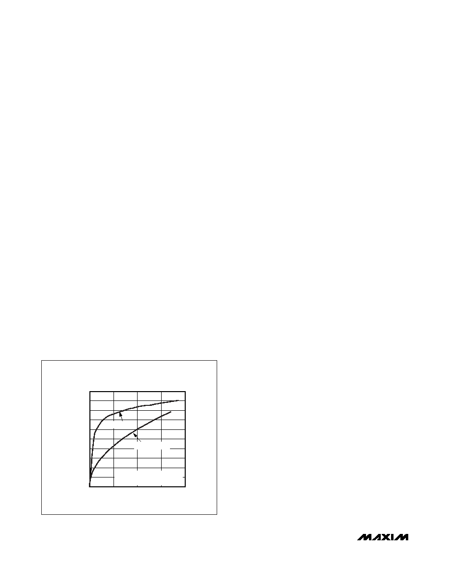
The theoretical best efficiency of a linear amplifier is
78%, however, that efficiency is only exhibited at peak
output power. Under normal operating levels (typical
music reproduction levels), efficiency falls below 30%,
whereas the MAX9877 still exhibits 70% efficiency
under the same conditions (Figure 3).
Ultra-Low EMI Filterless Output Stage
In traditional Class D amplifiers, the high dV/dt of the
rising and falling edge transitions results in increased
EMI emissions, which requires the use of external LC
filters or shielding to meet EN55022 electromagnetic-
interference (EMI) regulation standards. Limiting the
dV/dt normally results in decreased efficiency. Maxim’s
active emissions limiting circuitry actively limits the
dV/dt of the rising and falling edge transitions, provid-
ing reduced EMI emissions, while maintaining up to
87% efficiency.
In addition to active emission limiting, the MAX9877
features a spread-spectrum modulation mode that flat-
tens the wideband spectral components. Proprietary
techniques ensure that the cycle-to-cycle variation of
the switching period does not degrade audio reproduc-
tion or efficiency (see the
Typical Operating
Characteristics). Select spread-spectrum modulation
mode through the I2C interface (Table 6). In spread-
spectrum modulation mode, the switching frequency
varies randomly by ±60kHz around the center frequen-
cy (1.176MHz). The effect is to reduce the peak energy
at harmonics of the switching frequency. Above
10MHz, the wideband spectrum looks like white noise
for EMI purposes (see Figure 4).
Speaker Current Limit
Most applications will not enter current limit unless the
output is short circuited or connected incorrectly.
When the output current of the speaker amplifier
exceeds the current limit (1.5A, typ) the MAX9877 dis-
ables the outputs for approximately 250s. At the end of
250s, the outputs are re-enabled, if the fault condition
still exists, the MAX9877 will continue to disable and re-
enable the outputs until the fault condition is removed.
Bypass Mode
The integrated DPST analog audio switch allows the
MAX9877’s Class D amplifier to be bypassed. In
bypass mode, the Class D amplifier is automatically
disabled allowing an external amplifier to drive the
speaker connected between OUT+ and OUT- through
RXIN+ and RXIN- (see the
Typical Application Circuit).
The bypass switch is enabled at startup. The switch can
be opened or closed even when the MAX9877 is in soft-
ware shutdown (see the
I2C Register Description section).
Unlike discrete solutions, the switch design reduces
coupling of Class D switching noise to the RXIN_
inputs. This eliminates the need for a costly T-switch.
The bypass switch is typically used with two 9.1Ω resis-
tors connected to each input. These resistors, in combi-
nation with the switch on-resistance and an 8Ω load,
approximate the 32Ω load expected by the external
amplifier. Although not required, using the resistors
optimizes THD+N.
Drive RXIN+ and RXIN- with a low-impedance source
to minimize noise on the pins. In applications that do
not require the bypass mode, leave RXIN+ and RXIN-
unconnected.
MAX9877 EFFICIENCY
vs. IDEAL CLASS EFFICIENCY
MAX9877
fig03
OUTPUT POWER (W)
EFFICIENCY
(%)
0.75
0.50
0.25
10
20
30
40
50
60
70
80
90
100
0
1.00
MAX9877
IDEAL CLASS AB
VDD = PVDD = 3.7V (MAX9877)
VSUPPLY = 3.7V (IDEAL CLASS AB)
Figure 3. MAX9877 Efficiency vs. Class AB Efficiency
相关PDF资料 |
PDF描述 |
|---|---|
| MAX9879ERV+T | IC AUDIO SUBSYSTEM 30-UCSP |
| MAX987EUK-T | IC COMP MICRPWR R-R I/O SOT23-5 |
| MAX9888EWY+T | IC CODEC AUDIO FLEXSOUND 63WLP |
| MAX9890AEBL+T | IC SUPP CLICK-POP 9-UCSP |
| MAX9892ELT+T | IC ELIMINATOR CLICK/POP 6UDFN |
相关代理商/技术参数 |
参数描述 |
|---|---|
| MAX9879ERV+T | 功能描述:音频放大器 Audio Subsystem w/DirectDrive RoHS:否 制造商:STMicroelectronics 产品:General Purpose Audio Amplifiers 输出类型:Digital 输出功率: THD + 噪声: 工作电源电压:3.3 V 电源电流: 最大功率耗散: 最大工作温度: 安装风格:SMD/SMT 封装 / 箱体:TQFP-64 封装:Reel |
| MAX9879EVKIT+ | 功能描述:音频放大器 Stereo Class D Audio Subsystem with DirectDrive Headphone Amplifier RoHS:否 制造商:STMicroelectronics 产品:General Purpose Audio Amplifiers 输出类型:Digital 输出功率: THD + 噪声: 工作电源电压:3.3 V 电源电流: 最大功率耗散: 最大工作温度: 安装风格:SMD/SMT 封装 / 箱体:TQFP-64 封装:Reel |
| MAX987ESA | 功能描述:校验器 IC Single uPower Comparator RoHS:否 制造商:STMicroelectronics 产品: 比较器类型: 通道数量: 输出类型:Push-Pull 电源电压-最大:5.5 V 电源电压-最小:1.1 V 补偿电压(最大值):6 mV 电源电流(最大值):1350 nA 响应时间: 最大工作温度:+ 125 C 安装风格:SMD/SMT 封装 / 箱体:SC-70-5 封装:Reel |
| MAX987ESA+ | 功能描述:校验器 IC Single uPower Comparator RoHS:否 制造商:STMicroelectronics 产品: 比较器类型: 通道数量: 输出类型:Push-Pull 电源电压-最大:5.5 V 电源电压-最小:1.1 V 补偿电压(最大值):6 mV 电源电流(最大值):1350 nA 响应时间: 最大工作温度:+ 125 C 安装风格:SMD/SMT 封装 / 箱体:SC-70-5 封装:Reel |
| MAX987ESA+T | 功能描述:校验器 IC Single uPower Comparator RoHS:否 制造商:STMicroelectronics 产品: 比较器类型: 通道数量: 输出类型:Push-Pull 电源电压-最大:5.5 V 电源电压-最小:1.1 V 补偿电压(最大值):6 mV 电源电流(最大值):1350 nA 响应时间: 最大工作温度:+ 125 C 安装风格:SMD/SMT 封装 / 箱体:SC-70-5 封装:Reel |
发布紧急采购,3分钟左右您将得到回复。