参数资料
| 型号: | MAX9916EKA+T |
| 厂商: | Maxim Integrated Products |
| 文件页数: | 12/12页 |
| 文件大小: | 0K |
| 描述: | IC OP AMP RRIO SOT23-8 |
| 产品培训模块: | Lead (SnPb) Finish for COTS Obsolescence Mitigation Program |
| 标准包装: | 1 |
| 放大器类型: | 通用 |
| 电路数: | 2 |
| 输出类型: | 满摆幅 |
| 转换速率: | 0.5 V/µs |
| 增益带宽积: | 1MHz |
| 电流 - 输入偏压: | 1pA |
| 电压 - 输入偏移: | 200µV |
| 电流 - 电源: | 40µA |
| 电流 - 输出 / 通道: | 15mA |
| 电压 - 电源,单路/双路(±): | 1.8 V ~ 5.5 V |
| 工作温度: | -40°C ~ 85°C |
| 安装类型: | 表面贴装 |
| 封装/外壳: | SOT-23-8 |
| 供应商设备封装: | SOT-23-8 |
| 包装: | 标准包装 |
| 产品目录页面: | 1392 (CN2011-ZH PDF) |
| 其它名称: | MAX9916EKA+TDKR |
Detailed Description
Featuring a maximized ratio of gain bandwidth to
supply current, low operating supply voltage, low input
bias current, and rail-to-rail inputs and outputs, the
MAX9914–MAX9917 are an excellent choice for preci-
sion or general-purpose low-current, low-voltage, bat-
tery-powered applications. These CMOS devices
consume an ultra-low 20A (typ) supply current and a
200V (typ) offset voltage. For additional power
conservation, the MAX9914/MAX9917 feature a low-
power shutdown mode that reduces supply current to
1nA (typ), and puts the amplifiers’ output in a high-
impedance state. These devices are unity-gain stable
with a 1MHz gain-bandwidth product driving capacitive
loads up to 30pF. The capacitive load can be
increased to 100pF when the amplifier is configured for
a 10V/V gain.
Rail-to-Rail Inputs and Outputs
The MAX9914–MAX9917 amplifiers all have a parallel-
connected n- and p-channel differential input stage that
allows an input common-mode voltage range that
extends 100mV beyond the positive and negative sup-
ply rails, with excellent common-mode rejection.
The MAX9914–MAX9917 are capable of driving the out-
put to within 5mV of both supply rails with a 100k
Ω load.
These devices can drive a 5k
Ω load with swings to within
60mV of the rails. Figure 1 shows no clipping at the out-
put voltage swing of the MAX9914–MAX9917 configured
as a unity-gain buffer powered from a single 3V supply.
Low Input Bias Current
The MAX9914–MAX9917 feature ultra-low 1pA (typ)
input bias current. The variation in the input bias
current is minimal with changes in the input voltage due
to very high input impedance (in the order of 1G
Ω).
Applications Information
Driving Capacitive Loads
The MAX9914–MAX9917 amplifiers are unity-gain
stable for loads up to 30pF. However, the capacitive
load can be increased to 100pF when the amplifier is
configured for a minimum gain of 10V/V.
Applications that require greater capacitive drive
capability should use an isolation resistor between the
output and the capacitive load (Figure 2). Also, in
unity-gain applications with relatively small RL (about
5k
Ω), the capacitive load can be increased up to 100pF.
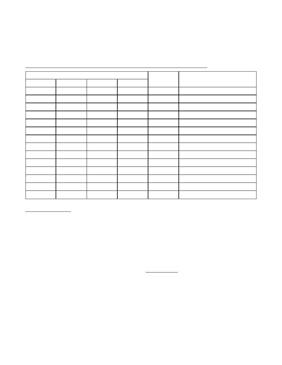
PIN
MAX9914
MAX9915
MAX9916
MAX9917
NAME
FUNCTION
1
—
IN+
Noninverting Amplifier Input
224
4
VSS
Negative Supply Voltage
3
—
IN-
Inverting Amplifier Input
4
—
OUT
Amplifier Output
568
10
VDD
Positive Supply Voltage
—5
—
SHDN
Shutdown
—
1
OUTA
Amplifier Output Channel A
—
2
INA-
Inverting Amplifier Input Channel A
—
3
INA+
Noninverting Amplifier Input Channel A
———
5
SHDNA
Shutdown Channel A
———
6
SHDNB
Shutdown Channel B
—
5
7
INB+
Noninverting Amplifier Input Channel B
—
6
8
INB-
Inverting Amplifier Input Channel B
—
7
9
OUTB
Amplifier Output Channel B
Pin Description
MAX9914–MAX9917
1MHz, 20A, Rail-to-Rail
I/O Op Amps with Shutdown
9
Maxim Integrated
相关PDF资料 |
PDF描述 |
|---|---|
| RC0805FR-07261KL | RES 261K OHM 1/8W 1% 0805 SMD |
| MAX9912EKA+T | IC OP AMP R-R I/O SOT23-8 |
| RC0805FR-0722K6L | RES 22.6K OHM 1/8W 1% 0805 SMD |
| FI-J20S-VF15N | CONN RCPT 0.4MM 20POS VERT SMD |
| RC0805FR-0722KL | RES 22.0K OHM 1/8W 1% 0805 SMD |
相关代理商/技术参数 |
参数描述 |
|---|---|
| MAX9916EUA | 制造商:Maxim Integrated Products 功能描述:- Rail/Tube |
| MAX9916EUA+ | 制造商:Maxim Integrated Products 功能描述:- Rail/Tube |
| MAX9916EUA+T | 制造商:Maxim Integrated Products 功能描述:OP AMP DUAL GP R-R I/O 6V 8PIN UMAX - Tape and Reel |
| MAX9916EUA-T | 制造商:Maxim Integrated Products 功能描述:- Tape and Reel |
| MAX9917EUB | 功能描述:运算放大器 - 运放 RoHS:否 制造商:STMicroelectronics 通道数量:4 共模抑制比(最小值):63 dB 输入补偿电压:1 mV 输入偏流(最大值):10 pA 工作电源电压:2.7 V to 5.5 V 安装风格:SMD/SMT 封装 / 箱体:QFN-16 转换速度:0.89 V/us 关闭:No 输出电流:55 mA 最大工作温度:+ 125 C 封装:Reel |
发布紧急采购,3分钟左右您将得到回复。