参数资料
| 型号: | MAX9916EKA+T |
| 厂商: | Maxim Integrated Products |
| 文件页数: | 5/12页 |
| 文件大小: | 0K |
| 描述: | IC OP AMP RRIO SOT23-8 |
| 产品培训模块: | Lead (SnPb) Finish for COTS Obsolescence Mitigation Program |
| 标准包装: | 1 |
| 放大器类型: | 通用 |
| 电路数: | 2 |
| 输出类型: | 满摆幅 |
| 转换速率: | 0.5 V/µs |
| 增益带宽积: | 1MHz |
| 电流 - 输入偏压: | 1pA |
| 电压 - 输入偏移: | 200µV |
| 电流 - 电源: | 40µA |
| 电流 - 输出 / 通道: | 15mA |
| 电压 - 电源,单路/双路(±): | 1.8 V ~ 5.5 V |
| 工作温度: | -40°C ~ 85°C |
| 安装类型: | 表面贴装 |
| 封装/外壳: | SOT-23-8 |
| 供应商设备封装: | SOT-23-8 |
| 包装: | 标准包装 |
| 产品目录页面: | 1392 (CN2011-ZH PDF) |
| 其它名称: | MAX9916EKA+TDKR |
MAX9914–MAX9917
1MHz, 20A, Rail-to-Rail
I/O Op Amps with Shutdown
2
Maxim Integrated
ABSOLUTE MAXIMUM RATINGS
Stresses beyond those listed under “Absolute Maximum Ratings” may cause permanent damage to the device. These are stress ratings only, and functional
operation of the device at these or any other conditions beyond those indicated in the operational sections of the specifications is not implied. Exposure to
absolute maximum rating conditions for extended periods may affect device reliability.
Power-Supply Voltage (VDD to VSS) ......................-0.3V to +6.0V
IN_+, IN_-, OUT_, SHDN_............... (VSS - 0.3V) to (VDD + 0.3V)
Current into IN_+, IN_- ......................................................
±20mA
Output Short-Circuit Duration to VDD or VSS ..............Continuous
Continuous Power Dissipation (TA = +70
°C)
5-Pin SC70 (derate 3.1mW/
°C above +70°C)............. 247mW
6-Pin SC70 (derate 3.1mW/
°C above +70°C)............. 245mW
8-Pin SOT23 (derate 9.1mW/
°C above +70°C)........... 727mW
10-Pin MAX (derate 5.6mW/
°C above +70°C) ...........444mW
Operating Temperature Range .......................... -40
°C to +85°C
Junction Temperature .....................................................+150
°C
Storage Temperature Range ............................-65
°C to +150°C
Lead Temperature (soldering, 10s) ............................... +300
°C
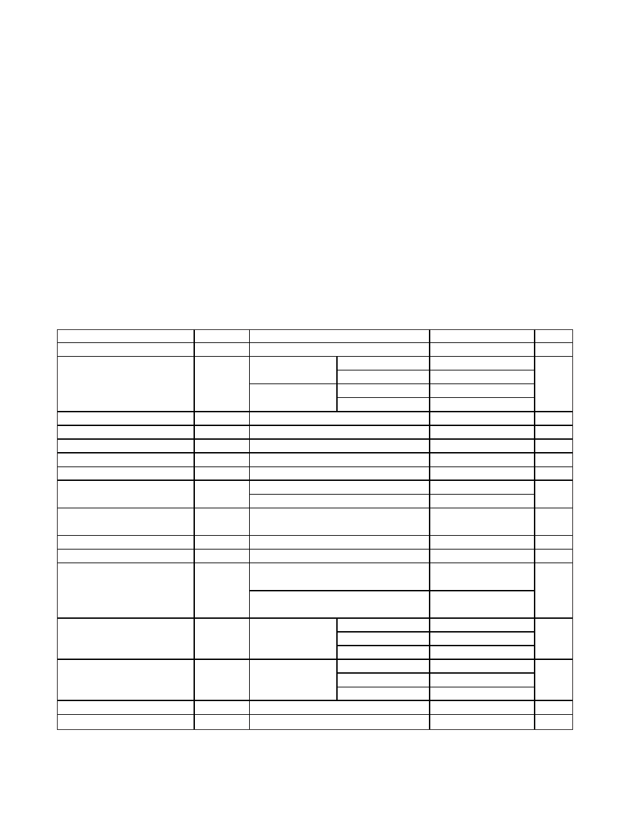
ELECTRICAL CHARACTERISTICS
(VDD = 1.8V to 5.5V, VSS = 0V, VCM = 0V, VOUT = VDD / 2, RL =
∞ connected to VDD / 2, SHDN_ = VDD, TA = +25°C, unless otherwise
noted.) (Note 1)
PARAMETER
SYMBOL
CONDITIONS
MIN
TYP
MAX
UNITS
Supply Voltage Range
VDD
Guaranteed by PSRR test
1.8
5.5
V
VDD = 1.8V
20
MAX9914/MAX9915
VDD = 5.5V
20
25
VDD = 1.8V
40
Supply Current
IDD
MAX9916/MAX9917
VDD = 5.5V
40
50
A
Shutdown Supply Current
IDD(SHDN_)
SHDN_ = GND, MAX9915/MAX9917
0.001
0.5
A
Input Offset Voltage
VOS
±0.2
±1mV
Input-Offset-Voltage Matching
MAX9916/MAX9917
±250
V
Input Bias Current
IB
(Note 2)
±1
±10
pA
Input Offset Current
IOS
(Note 2)
±1
±10
pA
Common mode
1
Input Resistance
RIN
Differential mode, -1mV < VIN < +1mV
10
G
Ω
Input Common-Mode Range
VCM
Guaranteed by CMRR test
VSS -
0.1
VDD +
0.1
V
Common-Mode Rejection Ratio
CMRR
-0.1V < VCM < VDD + 0.1V, VDD = 5.5V
70
80
dB
Power-Supply Rejection Ratio
PSRR
1.8V < VDD < 5.5V
65
85
dB
25mV < VOUT < VDD - 25mV,
RL = 100k
Ω, VDD = 5.5V
95
120
Open-Loop Gain
AVOL
100mV < VOUT < VDD - 100mV,
RL = 5k
Ω, VDD = 5.5V
95
110
dB
RL = 100k
Ω
2.5
5
RL = 5k
Ω
50
70
Output-Voltage-Swing High
VOH
VDD - VOUT
RL = 1k
Ω
250
mV
RL = 100k
Ω
2.5
5
RL = 5k
Ω
50
70
Output-Voltage-Swing Low
VOL
VOUT - VSS
RL = 1k
Ω
250
mV
Channel-to-Channel Isolation
CHISO
Specified at DC, MAX9916/MAX9917
100
dB
Output Short-Circuit Current
IOUT(SC)
±15
mA
相关PDF资料 |
PDF描述 |
|---|---|
| RC0805FR-07261KL | RES 261K OHM 1/8W 1% 0805 SMD |
| MAX9912EKA+T | IC OP AMP R-R I/O SOT23-8 |
| RC0805FR-0722K6L | RES 22.6K OHM 1/8W 1% 0805 SMD |
| FI-J20S-VF15N | CONN RCPT 0.4MM 20POS VERT SMD |
| RC0805FR-0722KL | RES 22.0K OHM 1/8W 1% 0805 SMD |
相关代理商/技术参数 |
参数描述 |
|---|---|
| MAX9916EUA | 制造商:Maxim Integrated Products 功能描述:- Rail/Tube |
| MAX9916EUA+ | 制造商:Maxim Integrated Products 功能描述:- Rail/Tube |
| MAX9916EUA+T | 制造商:Maxim Integrated Products 功能描述:OP AMP DUAL GP R-R I/O 6V 8PIN UMAX - Tape and Reel |
| MAX9916EUA-T | 制造商:Maxim Integrated Products 功能描述:- Tape and Reel |
| MAX9917EUB | 功能描述:运算放大器 - 运放 RoHS:否 制造商:STMicroelectronics 通道数量:4 共模抑制比(最小值):63 dB 输入补偿电压:1 mV 输入偏流(最大值):10 pA 工作电源电压:2.7 V to 5.5 V 安装风格:SMD/SMT 封装 / 箱体:QFN-16 转换速度:0.89 V/us 关闭:No 输出电流:55 mA 最大工作温度:+ 125 C 封装:Reel |
发布紧急采购,3分钟左右您将得到回复。