- 您现在的位置:买卖IC网 > PDF目录2159 > MAX9929FAUA+T (Maxim Integrated Products)IC AMP CURRENT SENSE 8-UMAX PDF资料下载
参数资料
| 型号: | MAX9929FAUA+T |
| 厂商: | Maxim Integrated Products |
| 文件页数: | 13/14页 |
| 文件大小: | 0K |
| 描述: | IC AMP CURRENT SENSE 8-UMAX |
| 产品培训模块: | Lead (SnPb) Finish for COTS Obsolescence Mitigation Program |
| 标准包装: | 2,500 |
| 放大器类型: | 电流检测 |
| 电路数: | 1 |
| -3db带宽: | 150kHz |
| 电流 - 输入偏压: | 1.6µA |
| 电压 - 输入偏移: | 6000µV |
| 电流 - 电源: | 20µA |
| 电压 - 电源,单路/双路(±): | 2.5 V ~ 5.5 V |
| 工作温度: | -40°C ~ 125°C |
| 安装类型: | 表面贴装 |
| 封装/外壳: | 8-TSSOP,8-MSOP(0.118",3.00mm 宽) |
| 供应商设备封装: | 8-uMAX |
| 包装: | 带卷 (TR) |
MAX9928/MAX9929
-0.1V to +28V Input Range, Micropower,
Uni-/Bidirectional, Current-Sense Amplifiers
8
_______________________________________________________________________________________
Detailed Description
The MAX9928F/MAX9929F micropower uni-/bidirectional,
current-sense amplifiers feature -0.1V to +28V input
common-mode range that is independent of the supply
voltage. This wide input voltage range feature allows the
monitoring of the current flow out of a power supply dur-
ing short-circuit/fault conditions, and also enables high-
side current sensing at voltages far in excess of the
supply voltage (VCC). The MAX9928F/MAX9929F oper-
ate from a 2.5V to 5.5V single supply and draw a low
20A quiescent supply current.
Current flows through the sense resistor, generating a
sense voltage VSENSE (Figure 1). The comparator sens-
es the direction of the sense voltage and configures the
amplifier for either positive or negative sense voltages
by controlling the S1 and S2 switches.
For positive VSENSE voltage, the amplifier’s inverting
input is high impedance and equals VIN - VSENSE. The
amplifier’s output drives the base of Q1, forcing its non-
inverting input terminal to (VIN - VSENSE); this causes a
current to flow through RG1 equal to |VSENSE|/RG1.
Transistor Q2 and the current mirror amplify the current
by a factor of M.
For negative VSENSE voltage, the amplifier’s noninvert-
ing input is high impedance and the voltage on RS- ter-
minal equals VIN + VSENSE. The amplifier’s output
drives the base of Q1 forcing its inverting input terminal
to match the voltage at the noninverting input terminal;
this causes a current to flow through RG2 equal to
|VSENSE|/RG2. Again, transistor Q2 and the current mir-
ror amplify the current by a factor of M.
+VSENSE vs. -VSENSE
The amplifier is configured for either positive VSENSE or
negative VSENSE by the SIGN comparator. The com-
parator has a built-in offset skew of -1.2mV so that ran-
dom offsets in the comparator do not affect the
precision of IOUT (VOUT) with positive VSENSE. The
comparator has a small amount of hysteresis (typically
0.6mV) to prevent its output from oscillating at the
crossover sense voltage. The ideal transfer characteris-
tic of IOUT (VOUT) and the output of the comparator
(SIGN) is shown in Figure 2.
The amplifier VOS is only trimmed for the positive VSENSE
voltages (VRS+ > VRS-). The SIGN comparator reconfig-
ures the internal structure of the amplifier to work with
negative VSENSE voltages (VRS- > VRS+) and the preci-
sion VOS trim is no longer effective and the resulting VOS
is slightly impacted. See details in the
Electrical
Characteristics Note 2. The user can choose the direc-
tion that needs the best precision to be the direction
where VRS+ > VRS-. For example, when monitoring Li+
battery currents, the discharge current should be VRS+ >
VRS- to give the best accuracy over the largest dynamic
range. When the battery charger is plugged in, the
charge current flows in the opposite direction and is
usually much larger, and a higher VOS error can be
tolerated. See the
Typical Operating Circuit.
For applications with unidirectional currents (e.g., bat-
tery discharge only), the SIGN output can be ignored.
Note that as VSENSE increases, the output current (IOUT
for the MAX9928 or VOUT/10kΩ for the MAX9929) also
increases. This additional current is supplied from VCC.
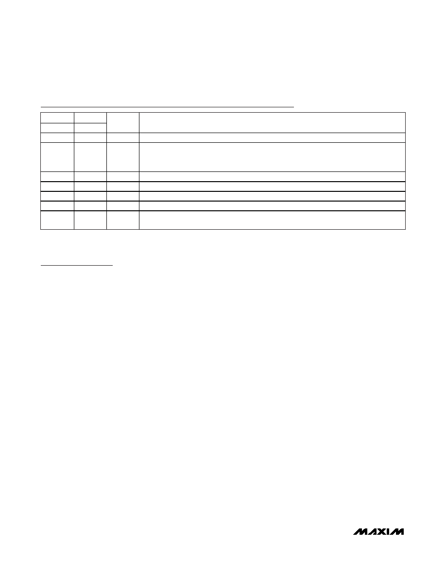
Pin/Bump Description
PIN
BUMP
MAX
UCSP
NAME
FUNCTION
1
B3
RS-
Negative Current-Sense Input. Load-side connection for the external sense resistor.
2
B2
SIGN
SIGN Output. Indicates polarity of VSENSE.
SIGN = H indicates VRS+ > VRS-
SIGN = L indicates VRS+ < VRS-
3
B1
RS+
Positive Current-Sense Input. Power-side connection to the external sense resistor.
4, 5
—
N.C.
No Connection. Not internally connected.
6A1
VCC
Supply Voltage Input. Bypass to GND with a 0.1F capacitor.
7
A2
GND
Circuit Ground
8
A3
OUT
Current-Sense Output. MAX9928: Current output (IOUT is proportional to |VSENSE|). MAX9929:
Voltage output (VOUT is proportional to |VSENSE|).
相关PDF资料 |
PDF描述 |
|---|---|
| MAX9934TALT+T | IC AMP CURR SENSE LV 6UDFN |
| MAX9937AXK+T | IC AMP CURRENT SENSE SC70-5 |
| MAX9938WEUK+T | IC AMP CURRENT SENSE SOT23-5 |
| MAX9939AUB+T | IC AMP PGA SPI VOS I/O 10MSOP |
| MAX9943AUA+T | IC OPAMP PREC LP/HV SGL 8-MSOP |
相关代理商/技术参数 |
参数描述 |
|---|---|
| MAX9929TABS+TG45 | 制造商:Maxim Integrated Products 功能描述:0V TO 28V CMR ISENSE - Tape and Reel |
| MAX9929TAUA+T | 制造商:Maxim Integrated Products 功能描述:- Tape and Reel |
| MAX992EKA | 制造商:Maxim Integrated Products 功能描述:HIGH-SPEED MICROPOWER LOW-VOLTAGE - Cut Tape Product |
| MAX992EKA+ | 制造商:Maxim Integrated Products 功能描述:COMPARATOR DUAL R-R I/O 2.75V/5.5V 8PIN SOT-23 - Rail/Tube |
| MAX992EKA+T | 功能描述:校验器 IC Dual uPower Comparator RoHS:否 制造商:STMicroelectronics 产品: 比较器类型: 通道数量: 输出类型:Push-Pull 电源电压-最大:5.5 V 电源电压-最小:1.1 V 补偿电压(最大值):6 mV 电源电流(最大值):1350 nA 响应时间: 最大工作温度:+ 125 C 安装风格:SMD/SMT 封装 / 箱体:SC-70-5 封装:Reel |
发布紧急采购,3分钟左右您将得到回复。