- 您现在的位置:买卖IC网 > PDF目录2159 > MAX9929FAUA+T (Maxim Integrated Products)IC AMP CURRENT SENSE 8-UMAX PDF资料下载
参数资料
| 型号: | MAX9929FAUA+T |
| 厂商: | Maxim Integrated Products |
| 文件页数: | 9/14页 |
| 文件大小: | 0K |
| 描述: | IC AMP CURRENT SENSE 8-UMAX |
| 产品培训模块: | Lead (SnPb) Finish for COTS Obsolescence Mitigation Program |
| 标准包装: | 2,500 |
| 放大器类型: | 电流检测 |
| 电路数: | 1 |
| -3db带宽: | 150kHz |
| 电流 - 输入偏压: | 1.6µA |
| 电压 - 输入偏移: | 6000µV |
| 电流 - 电源: | 20µA |
| 电压 - 电源,单路/双路(±): | 2.5 V ~ 5.5 V |
| 工作温度: | -40°C ~ 125°C |
| 安装类型: | 表面贴装 |
| 封装/外壳: | 8-TSSOP,8-MSOP(0.118",3.00mm 宽) |
| 供应商设备封装: | 8-uMAX |
| 包装: | 带卷 (TR) |
MAX9928/MAX9929
-0.1V to +28V Input Range, Micropower,
Uni-/Bidirectional, Current-Sense Amplifiers
4
_______________________________________________________________________________________
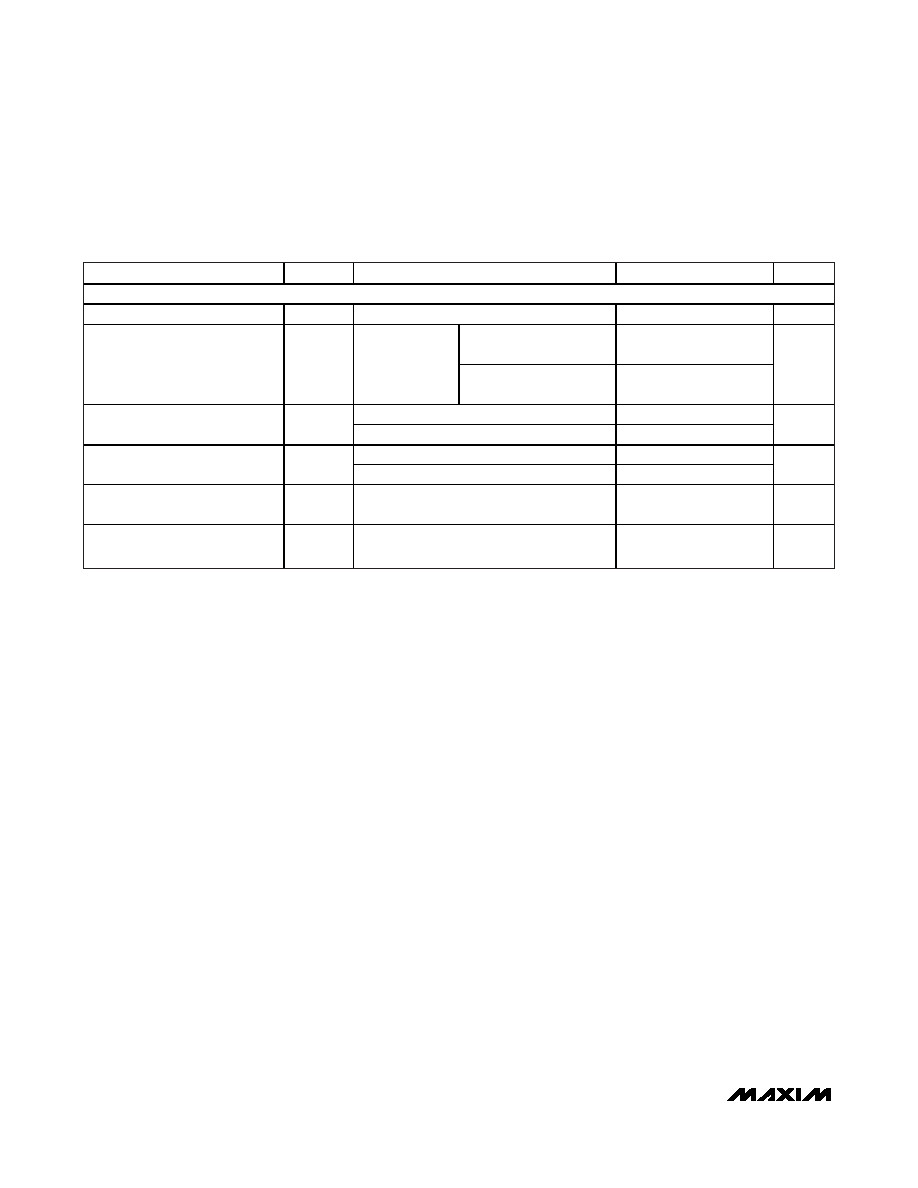
ELECTRICAL CHARACTERISTICS (continued)
(VRS+ = -0.1V to +28V, VCC = 3.3V, VSENSE = (VRS+ - VRS-) = 0V, ROUT = 10kΩ for MAX9928F, TA = -40°C to +125°C, unless other-
wise noted. Typical values are at TA = +25°C.) (Note 1)
PARAMETER
SYMBOL
CONDITIONS
MIN
TYP
MAX
UNITS
AC ELECTRICAL CHARACTERISTICS
-3dB Bandwidth
BW
MAX992_F, VSENSE = 50mV
150
kHz
MAX992_F, VSENSE =
5mV to 50mV step
6
OUT Settling to 1% of Final Value
tSET
VRS+ = 3.6V,
CLOAD = 10pF,
ROUT = 10k
Ω for
MAX9928F
MAX992_F, VSENSE =
50mV to 5mV step
15
s
Overdrive = 1mV
80
SIGN Comparator Propagation
Delay (Low to High)
tPROP_LH
Overdrive = 5mV
30
s
Overdrive = 1mV
50
SIGN Comparator Propagation
Delay (High to Low)
tPROP_HL
Overdrive = 5mV
13
s
Power-Up Time to 1% of Final
Value
VSENSE = 50mV for MAX992_F,
VRS+ = 3.6V, CLOAD = 10pF
50
s
Saturation Recovery Time
100mV
≤ VSENSE ≤ 50mV for MAX992_F,
VRS+ = 3.6V, CLOAD = 10pF
4ms
Note 1: All devices are 100% production tested at TA = +25°C. All temperature limits are guaranteed by design.
Note 2: VOS is extrapolated from two point transconductance and gain accuracy tests. Measurements are made at VSENSE =
+5mV and VSENSE = +50mV for MAX992_F. These measurements are also used to test the full-scale sense voltage,
transconductance, and gain. These VOS specifications are for the trimmed direction only (VRS+ > VRS-). For current flowing
in the opposite direction (VRS- > VRS+), VOS is ±1mV (max) at +25°C and ±1.8mV (max) over temperature, when VRS+ is at
3.6V. See the
Detailed Description for more information.
Note 3: Guaranteed by common-mode rejection ratio. Extrapolated VOS as described in Note 2 is used to calculate common-mode
rejection ratio.
Note 4: Includes input bias current of SIGN comparator.
Note 5: Leakage in to RS+ or RS- when VCC = 0V. Includes input leakage current of SIGN comparator. This specification does not
add to the bias current.
Note 6: Output voltage should be 650mV below VCC to achieve full accuracy.
Note 7: IOL is the minimum output current in the VSENSE - IOUT transfer characteristics. VOL is the minimum output voltage in the
VSENSE - VOUT transfer characteristic.
Note 8: VSENSE voltage required to switch comparator.
Note 9: Discharge to charge trip point is functionally tested at VCM = -0.1V, +3.6V, and +28V.
Note 10: Guaranteed by PSRR test. Extrapolated VOS as described in Note 2 is used to calculate the power-supply rejection ratio.
VSENSE has to be such that the output voltage is 650mV below VCC to achieve full accuracy.
相关PDF资料 |
PDF描述 |
|---|---|
| MAX9934TALT+T | IC AMP CURR SENSE LV 6UDFN |
| MAX9937AXK+T | IC AMP CURRENT SENSE SC70-5 |
| MAX9938WEUK+T | IC AMP CURRENT SENSE SOT23-5 |
| MAX9939AUB+T | IC AMP PGA SPI VOS I/O 10MSOP |
| MAX9943AUA+T | IC OPAMP PREC LP/HV SGL 8-MSOP |
相关代理商/技术参数 |
参数描述 |
|---|---|
| MAX9929TABS+TG45 | 制造商:Maxim Integrated Products 功能描述:0V TO 28V CMR ISENSE - Tape and Reel |
| MAX9929TAUA+T | 制造商:Maxim Integrated Products 功能描述:- Tape and Reel |
| MAX992EKA | 制造商:Maxim Integrated Products 功能描述:HIGH-SPEED MICROPOWER LOW-VOLTAGE - Cut Tape Product |
| MAX992EKA+ | 制造商:Maxim Integrated Products 功能描述:COMPARATOR DUAL R-R I/O 2.75V/5.5V 8PIN SOT-23 - Rail/Tube |
| MAX992EKA+T | 功能描述:校验器 IC Dual uPower Comparator RoHS:否 制造商:STMicroelectronics 产品: 比较器类型: 通道数量: 输出类型:Push-Pull 电源电压-最大:5.5 V 电源电压-最小:1.1 V 补偿电压(最大值):6 mV 电源电流(最大值):1350 nA 响应时间: 最大工作温度:+ 125 C 安装风格:SMD/SMT 封装 / 箱体:SC-70-5 封装:Reel |
发布紧急采购,3分钟左右您将得到回复。